ADP3171 データシートの表示(PDF) - Analog Devices
部品番号
コンポーネント説明
メーカー
ADP3171 Datasheet PDF : 13 Pages
| |||
ADP3171
Power MOSFETs
Two external N-channel power MOSFETs must be selected for
use with the ADP3171, one for the main switch and one for the
synchronous switch. The main selection parameters for the power
MOSFETs are the threshold voltage (VGS(TH)), the ON resistance
(RDS(ON)), and the gate charge (QG). Logic level MOSFETs are
highly recommended. Only logic level MOSFETs with VGS ratings
higher than the absolute maximum value of VCC should be used.
The maximum output current IO(MAX) determines the RDS(ON)
requirement for the two power MOSFETs. When the ADP3171
is operating in continuous mode, the simplifying assumption
can be made that one of the two MOSFETs is always conduct-
ing the average load current. For VIN = 5 V and VOUT = 1.5 V,
the maximum duty ratio of the high-side FET is:
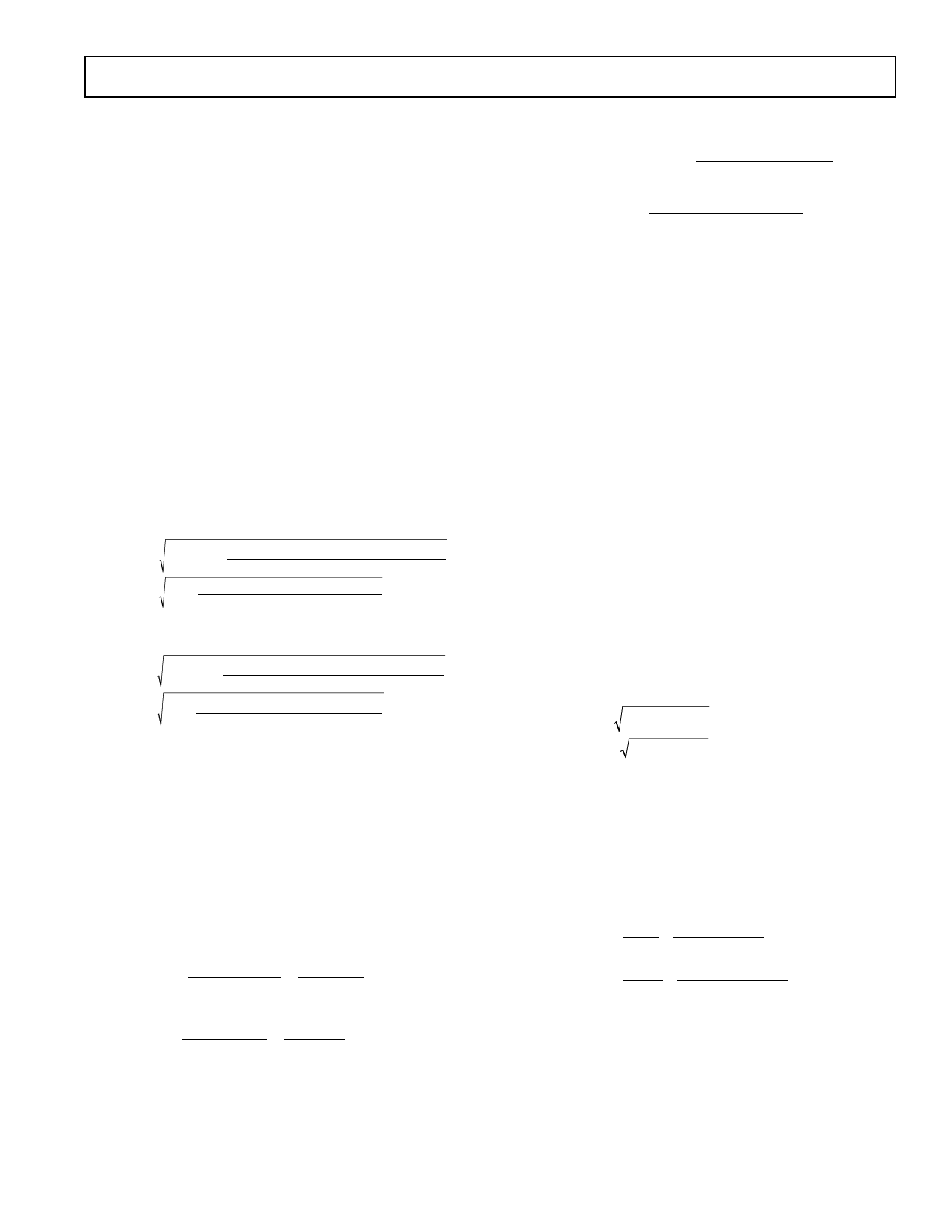
( ) DHSF ( MAX ) = 1 – fMIN + tOFF
( ) DHSF ( MAX ) = 1 – 192 kHz × 3.5 µs = 33%
(20)
The maximum duty ratio of the low-side (synchronous rectifier)
MOSFET is:
DLSF ( MAX ) = 1 – DHSF ( MAX ) = 67%
(21)
The maximum rms current of the high-side MOSFET is:
IHSF ( MAX ) =
IHSF ( MAX ) =
(22) DHSF ( MAX )
×
I2
L(VALLEY )
+ (IL(VALLEY )
3
×
IL(PEAK ) ) +
IL(PEAK
2
)
0.33 × 3.75 A2 + (3.75 A × 6.25 A) + 6.25 A2 = 2.9 A
3
The maximum rms current of the low-side MOSFET is:
ILSF ( MAX ) =
ILSF ( MAX ) =
(23) DLSF ( MAX )
×
IL(VALLEY
2
)
+ (IL(VALLEY ) ×
3
IL(PEAK ) ) +
IL
(
PEAK
2
)
)
( ) 3.75 A2 + (3.75 A × 6.25 A) + 6.25 A2
0.67 ×
= 4.1 A
3
The RDS(ON) for each MOSFET can be derived from the allowable
dissipation. If 10% of the maximum output power is allowed for
MOSFET dissipation, the total dissipation will be:
PD(FETs ) = 0.1 ×VOUT × IOUT ( MAX )
PD(FETs ) = 0.1 × 1.5V × 6.5 A = 975 mW
(24)
Allocating half of the total dissipation for the high-side MOSFET
and half for the low-side MOSFET, and assuming that the resistive
loss of the high-side MOSFET is one-third and the switching
loss is two-thirds of its total, the required maximum MOSFET
resistances will be:
RDS (ON )HSF
=
PD(FETs )
3
×
IHSF
(
MAX
2
)
=
975 mW
3 × 2.9 A2
= 38 mΩ
(25)
With this choice, the high-side MOSFET dissipation is:
PHSF
= RDS (ON )HSF
×
IHSF
(
MAX
2
)
+ VIN
× IL(PEAK ) × QG ×
2 × IG
fMIN
+VIN × QRR × fMIN
PHSF
= 35 mΩ × 2.9 A2
+
5 + 6.25 A × 12 nC
2×1A
× 192 kHz
+5V × 19 nC × 192 kHz = 349 mW
(27)
where the second term represents the turn-off loss of the MOSFET
and the third term represents the turn-on loss due to the stored
charge in the body diode of the low-side MOSFET. In the sec-
ond term, QG is the gate charge to be removed from the gate for
turn-off and IG is the gate turn-off current. From the data sheet,
the value of QG for the FDS6982 is 12 nC and the peak gate
drive current provided by the ADP3171 is about 1 A. In the
third term, QRR is the charge stored in the body diode of the
low-side MOSFET at the valley of the inductor current. The
data sheet of the FDS6982 shows a value of 19 nC for this
parameter.
The low-side MOSFET dissipation is:
PLSF
= RDS(ON )LSF
×
ILSF
(
MAX
2
)
PLSF = 22 mΩ × 4.1 A2 = 370 mW
(28)
Note that there are no switching losses in the low-side MOSFET.
CIN Selection and Input Current di/dt Reduction
In continuous inductor-current mode, the source current of the
high-side MOSFET is a square wave with a duty ratio of VOUT/VlN
and an amplitude of one-half of the maximum output current. To
prevent large voltage transients, a low ESR input capacitor sized
for the maximum rms current must be used. The maximum rms
capacitor current is given by:
IC(RMS ) = IO × DHSF – DHSF 2
IC(RMS ) = 5 A × 0.33 – 0.332 = 2.4 A
(29)
For a ZA-type capacitor with 1000 µF capacitance and 6.3 V
voltage rating, the ESR is 24 mΩ and the maximum allowable
ripple current at 100 kHz is 2 A. At 105°C, at least two such
capacitors should be connected in parallel to handle the calcu-
lated ripple current. At 50°C ambient, however, a higher ripple
current can be tolerated, so one capacitor is adequate.
The ripple voltage across the input capacitor is:
VC(RIPPLE )
= IO
×
ESRC
nC
+
nC
DHSF ( MAX )
× CIN × fMIN
VC(RIPPLE )
=
IO
×
24 mΩ
1
+
0.33
1 × 1 mF × 192 kHz
=
26
mV
(30)
RDS (ON )LSF
=
PD(FETs )
2
×
ILSF
(
MAX
2
)
= 975 mW
2 × 4.1 A2
= 29 mΩ
(26)
Note that there is a trade-off between converter efficiency and cost.
Larger MOSFETs reduce the conduction losses and allow higher
efficiency, but increase the system cost. A Fairchild FDB6982
dual MOSFET (high-side RDS(ON) = 28 mΩ nominal, 35 mΩ
worst-case; and low-side RDS(ON) = 16 mΩ nominal, 22 mΩ
worst-case) is a good choice in this application.
Linear Regulators
The linear regulators provide a low-cost, convenient, and versatile
solution for generating moderate current supply rails. The maxi-
mum output load current is determined by the size and thermal
impedance of the external N-channel power MOSFET that is
placed in series with the supply and controlled by the ADP3171.
The output voltage is sensed at the LRFB × pin and compared
to an internal reference voltage in a negative feedback loop that
keeps the output voltage in regulation. If the load is reduced or
REV. 0
–9–
Share Link: 