ADP5022 データシートの表示(PDF) - Analog Devices
部品番号
コンポーネント説明
メーカー
ADP5022 Datasheet PDF : 28 Pages
| |||
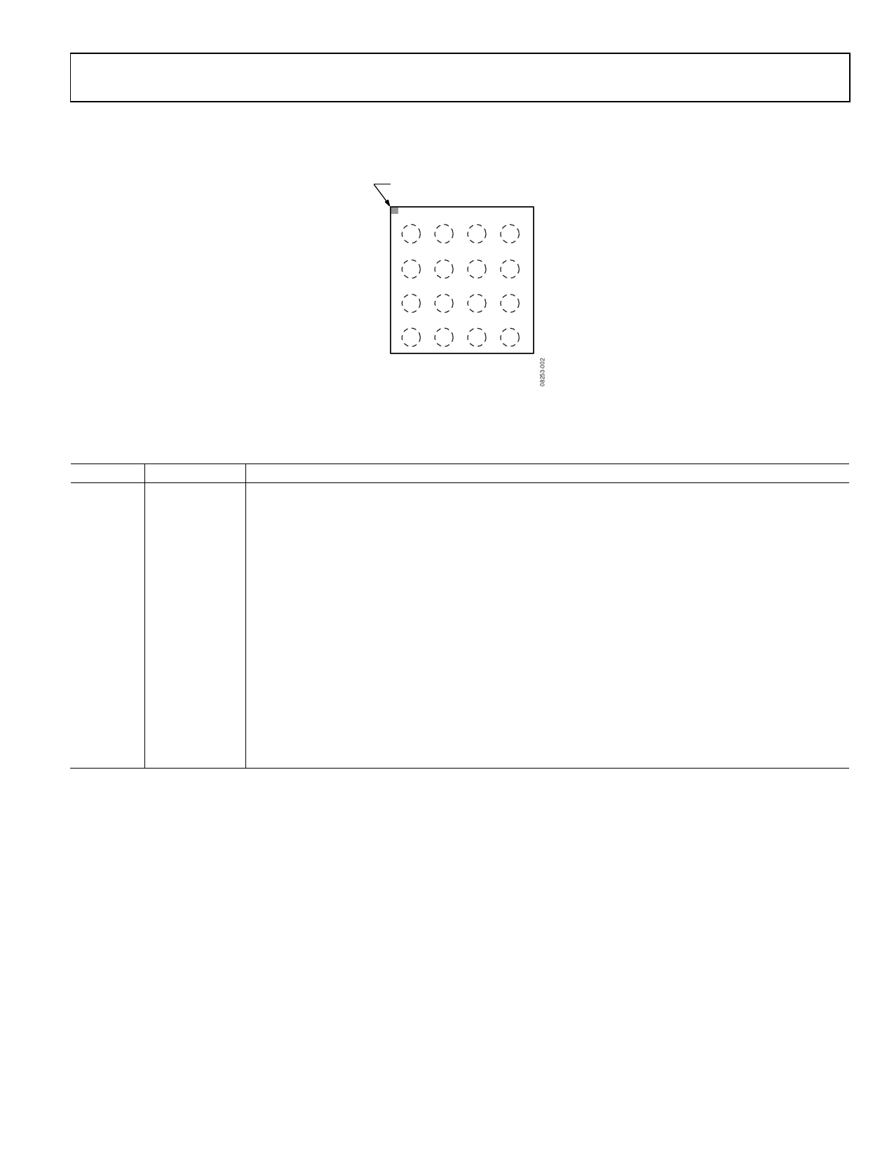
PIN CONFIGURATION AND FUNCTION DESCRIPTIONS
BALL A1
INDICATOR
1
2
3
4
VOUT3 AGND VIN3 VDDA
A
VIN1 EN1 EN2 VIN2
B
SW1 EN3 MODE SW2
C
PGND1 VOUT1 VOUT2 PGND2
D
TOP VIEW
(BALL SIDE DOWN)
Not to Scale
Figure 3. Pin Configuration
ADP5022
Table 6. Pin Function Descriptions
Pin No. Mnemonic
Description
A1
VOUT3
LDO Output Voltage and Sensing Input.
A2
AGND
Analog Ground.
A3
VIN3
LDO Input Supply (VIN3 ≤ VIN1 = VIN2 = VDDA).
A4
VDDA
Supply Input for the Housekeeping Block and UVLO Sensing.
B1
VIN1
Buck1 Input Supply (VIN1 = VIN2 = VDDA).
B2
EN1
Buck1 Activation. Set EN1 = high: turn on Buck1. Set EN1 = low: turn off Buck1.
B3
EN2
Buck2 Activation. Set EN2 = high: turn on Buck2. Set EN2 = low: turn off Buck2.
B4
VIN2
Buck2 Input Supply (VIN2 = VIN1 = VDDA).
C1
SW1
Buck1 Switching Node.
C2
EN3
LDO Activation. Set EN3 = high: turn on LDO. EN3 = low: turn off LDO.
C3
MODE
Buck1/Buck2 Operating Mode: MODE = high: forced PWM operation. MODE = low: auto PWM/PSM operation.
C4
SW2
Buck2 Switching Node.
D1
PGND1
Dedicated Power Ground for Buck1.
D2
VOUT1
Buck1 Output Voltage Sensing Input.
D3
VOUT2
Buck2 Output Voltage Sensing Input.
D4
PGND2
Dedicated Power Ground for Buck2.
Rev. C | Page 7 of 28
Share Link: 