ADR550ART-REEL7(RevA) データシートの表示(PDF) - Analog Devices
部品番号
コンポーネント説明
メーカー
ADR550ART-REEL7 Datasheet PDF : 16 Pages
| |||
ADR520/ADR525/ADR530/ADR540/ADR550
THEORY OF OPERATION
The ADR520/ADR525/ADR530/ADR540/ADR550 use the
band gap concept to produce a stable, low temperature
coefficient voltage reference suitable for high accuracy data
acquisition components and systems. The devices use the
physical nature of a silicon transistor base-emitter voltage in the
forward-biased operating region. All such transistors have
approximately a –2 mV/°C temperature coefficient (TC),
making them unsuitable for direct use as a low temperature
coefficient reference. Extrapolation of the temperature
characteristic of any one of these devices to absolute zero (with
the collector current proportional to the absolute temperature),
however, reveals that its VBE approaches approximately the
silicon band gap voltage. Thus, if a voltage develops with an
opposing temperature coefficient to sum the VBE, a zero
temperature coefficient reference results. The ADR5xx circuit
shown in Figure 18 provides such a compensating voltage (V1)
by driving two transistors at different current densities and
amplifying the resultant VBE difference (∆VBE, which has a
positive temperature coefficient). The sum of VBE and V1
provides a stable voltage reference over temperature.
+
V+
V1
• The RBIAS must be large enough so that IIN does not exceed
10 mA when the supply voltage is at its maximum value
and the load current is at its minimum value.
Given these conditions, the RBIAS is determined by the supply
voltage (VCC), the ADR5xx load and operating current (IL and
IQ), and the ADR5xx output voltage (VOUT).
RBIAS
=
VCC
IL
− VOUT
− IIN
(3)
VS
RBIAS
IIN
IIN + IL
VOUT
IL
ADR550
Figure 19. Shunt Reference
Precision Negative Voltage Reference
The ADR5xx is suitable for applications where a precise
negative voltage is desired. Figure 20 shows the ADR5xx
configured to provide a negative output.
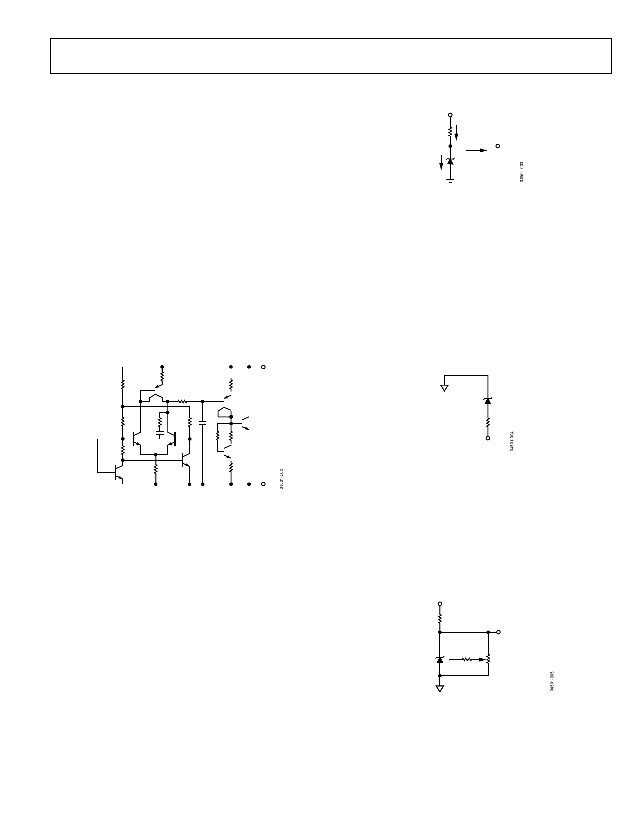
–
+
∆VBE
–
+
VBE
–
V–
Figure 18. Circuit Schematic
APPLICATIONS
The ADR520/ADR525/ADR530/ADR540/ADR550 are a series
of precision shunt voltage references. They are designed to
operate without an external capacitor between the positive and
negative terminals. If a bypass capacitor is used to filter the
supply, the references remains stable.
All shunt voltage references require an external bias resistor
(RBIAS) between the supply voltage and the reference (see
Figure 19). The RBIAS sets the current that flows through the load
(IL) and the reference (IIN). Because the load and the supply
voltage can vary, the RBIAS needs to be chosen based on the
following considerations:
• The RBIAS must be small enough to supply the minimum IIN
current to the ADR5xx, even when the supply voltage is at
its minimum value and the load current is at its maximum
value.
ADR525
RBIAS
–2.5V
VCC
Figure 20. Negative Precision Reference Configuration
Output Voltage Trim
The ADR5xx TRIM terminal can be used to adjust the output
voltage over a range of ±0.5%. This allows systems designers to
trim system errors by setting the reference to a voltage other
than the preset output voltage. An external mechanical or elec-
trical potentiometer can be used for this adjustment. Figure 21
illustrates how the output voltage can be trimmed by using the
AD5273, an Analog Devices 10 kΩ potentiometer.
VCC
RBIAS
ADR530
R1
470kΩ
VOUT
AD5273
POTENTIOMETER
10kΩ
Figure 21. Output Voltage Trim
Rev. A | Page 11 of 16
Share Link: 