ADT7463 データシートの表示(PDF) - ON Semiconductor
部品番号
コンポーネント説明
メーカー
ADT7463 Datasheet PDF : 52 Pages
| |||
ADT7463
SERIAL BUS INTERFACE
Control of the ADT7463 is carried out using the serial system
management bus (SMBus). The ADT7463 is connected to this
bus as a slave device, under the control of a master controller.
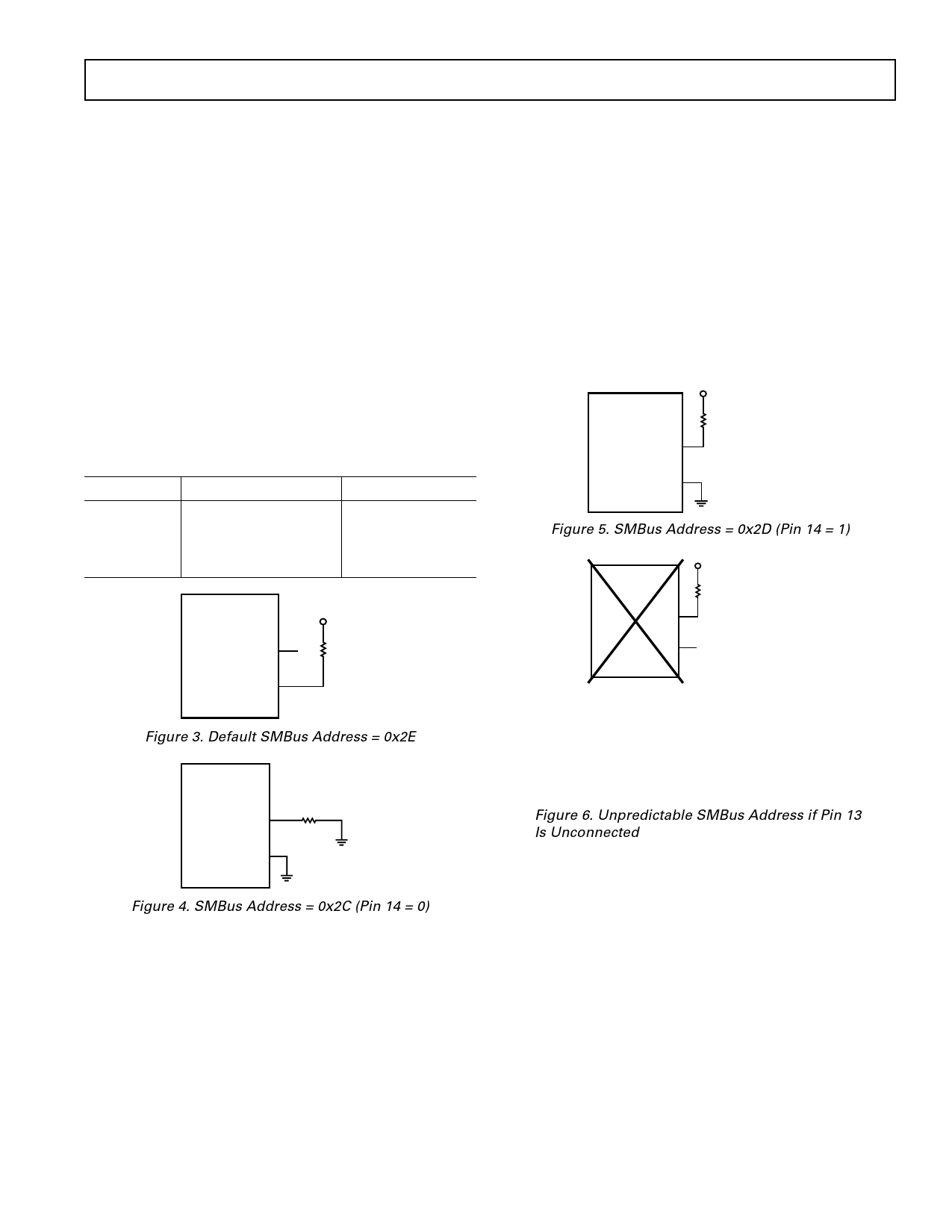
The ADT7463 has a 7-bit serial bus address. When the device
is powered up with Pin 13 (PWM3/ADDRESS ENABLE) high,
the ADT7463 has a default SMBus address of 0101110 or
0x2E. The read/write bit must be added to get the 8-bit address. If
more than one ADT7463 is used in a system, then each ADT7463
should be placed in address select mode by strapping Pin 13 low on
power-up. The logic state of Pin 14 then determines the device’s
SMBus address. The logic of these pins is sampled upon power-up.
The device address is sampled and latched on the first valid
SMBus transaction, more precisely on the low-to-high transition
at the beginning of the 8th SCL pulse, when the serial bus address
byte matches the selected slave address. The selected slave address
is chosen using the address enable/address select pins. Any
attempted changes in the address will have no effect after this.
Pin 13 State
0
0
1
Table I. Address Select Mode
Pin 14 State
Low (10 kΩ to GND)
High (10 kΩ Pull-Up)
Don’t Care
Address
0101100 (0x2C)
0101101 (0x2D)
0101110 (0x2E)
(Default)
ADT7463
VCC
14
ADDR_SEL
10k�
13
PWM3/ADDR_EN
ADDRESS = 0x2E
Figure 3. Default SMBus Address = 0x2E
ADT7463
14 10k�
ADDR_SEL
13
PWM3/ADDR_EN
ADDRESS = 0x2C
Figure 4. SMBus Address = 0x2C (Pin 14 = 0)
The ability to make hardwired changes to the SMBus slave
address allows the user to avoid conflicts with other devices sharing
the same serial bus, for example, if more than one ADT7463 is
used in a system.
The serial bus protocol operates as follows:
1. The master initiates data transfer by establishing a START
condition, defined as a high-to-low transition on the serial
data line SDA while the serial clock line SCL remains high.
This indicates that an address/data stream will follow. All
slave peripherals connected to the serial bus respond to the
START condition and shift in the next eight bits, consisting
of a 7-bit address (MSB first) plus a R/W bit, which deter-
mines the direction of the data transfer, i.e., whether data
will be written to or read from the slave device.
VCC
ADT7463
10k�
14
ADDR_SEL
PWM3/ADDR_EN 13
ADDRESS = 0x2D
Figure 5. SMBus Address = 0x2D (Pin 14 = 1)
VCC
ADT7463
10k�
14
ADDR_SEL
13
PWM3/ADDR_EN
NC
DO NOT LEAVE ADDR_EN
UNCONNECTED! CAN
CAUSE UNPREDICTABLE
ADDRESSES.
CARE SHOULD BE TAKEN TO ENSURE THAT PIN 13
(PWM3/ADDR_EN) IS EITHER TIED HIGH OR LOW. LEAVING PIN 13
FLOATING COULD CAUSE THE ADT7463 TO POWER UP WITH AN
UNEXPECTED ADDRESS.
NOTE THAT IF THE ADT7463 IS PLACED INTO ADDRESS SELECT
MODE, PINS 13 AND 14 CANNOT BE USED AS THE ALTERNATE
FUNCTIONS (PWM3, TACH4/THERM) ONLY IF THE CORRECT
CIRCUIT IS MUXED IN AT THE CORRECT TIME.
Figure 6. Unpredictable SMBus Address if Pin 13
Is Unconnected
The peripheral whose address corresponds to the transmitted
address responds by pulling the data line low during the low
period before the ninth clock pulse, known as the Acknowl-
edge Bit. All other devices on the bus now remain idle while
the selected device waits for data to be read from or written
to it. If the R/W bit is a 0, then the master writes to the
slave device. If the R/W bit is a 1, the master reads from
the slave device.
REV. C
Rev. 4 | Page 9 of 52 | www.onsemi.com
–9–
Share Link: 