ADT7470 データシートの表示(PDF) - Analog Devices
部品番号
コンポーネント説明
メーカー
ADT7470 Datasheet PDF : 40 Pages
| |||
ADT7470
Data Sheet
during the low period before the 10th clock pulse, then
high during the 10th clock pulse to assert a stop condition.
Any number of bytes of data can be transferred over the serial
bus in one operation. However, it is not possible to mix read
and write in one operation, because the type of operation is
determined at the beginning and subsequently cannot be
changed without starting a new operation.
In the ADT7470, write operations contain either one or two
bytes, and read operations contain one byte and perform the
following functions.
1
9
SCL
To write data to one of the device data registers or read data
from it, the address pointer register must be set so that the
correct data register is addressed. Then data can be written into
that register or read from it. The first byte of a write operation
always contains an address that is stored in the address pointer
register. If data is to be written to the device, the write operation
contains a second data byte that is written to the register selected
by the address pointer register.
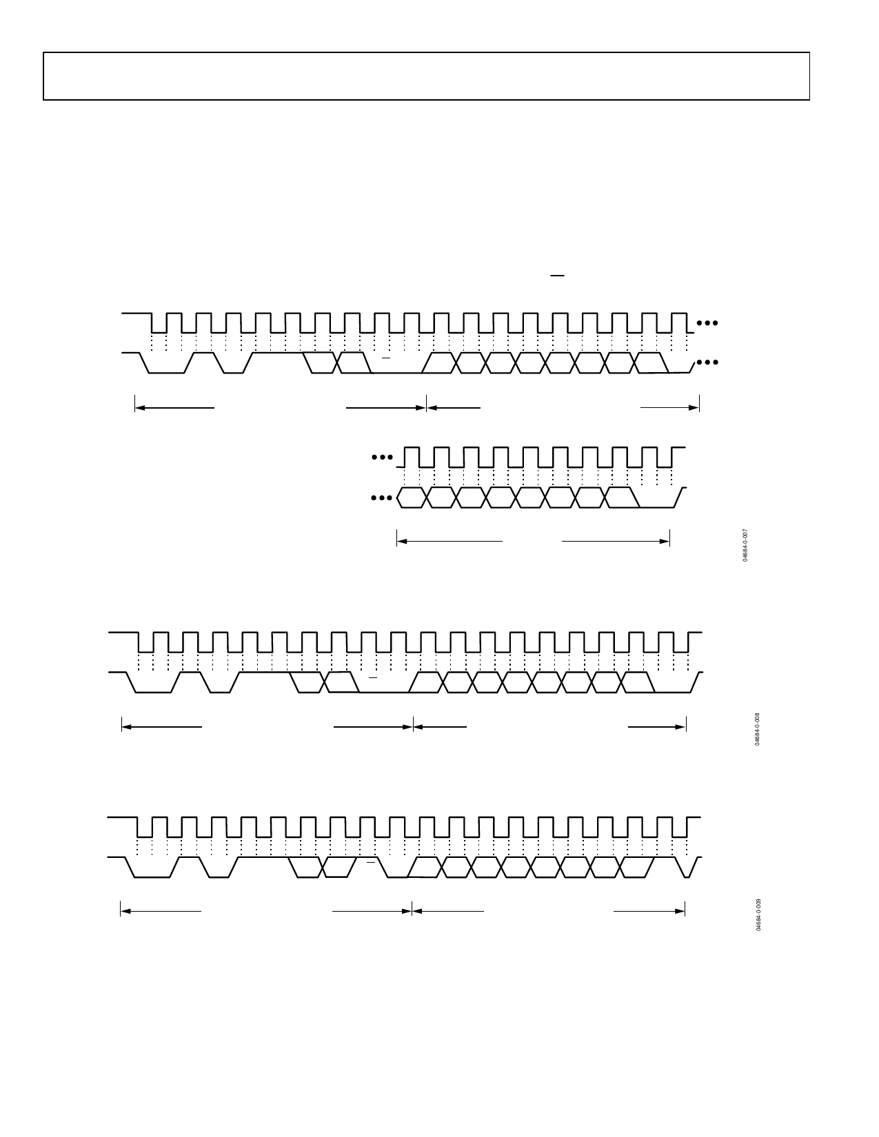
This is illustrated in Figure 7. The device address is sent over the
bus followed by R/W set to 0. This is followed by two data bytes.
1
9
SDA
0
1
START BY
MASTER
0
1
1 A1 A0 R/W
D7
FRAME 1
SERIAL BUS ADDRESS
BYTE
ACK. BY
ADT7470
1
SCL (CONTINUED)
D6 D5 D4 D3 D2 D1 D0
FRAME 2
ADDRESS POINTER REGISTER BYTE
ACK. BY
ADT7470
9
SDA (CONTINUED)
D7 D6 D5 D4 D3 D2 D1 D0
FRAME 3
DATA
BYTE
ACK. BY STOP BY
ADT7470 MASTER
Figure 7. Writing a Register Address to the Address Pointer Register, Then Writing Data to the Selected Register
1
9
1
9
SCL
SDA
0
1
START BY
MASTER
0
1
1
A1 A0 R/W
D7 D6 D5 D4 D3 D2 D1 D0
FRAME 1
SERIAL BUS ADDRESS
BYTE
ACK. BY
ADT7470
FRAME 2
ADDRESS POINTER REGISTER BYTE
Figure 8. Writing to the Address Pointer Register Only
ACK. BY STOP BY
ADT7470 MASTER
1
9
1
9
SCL
SDA
0
1
START BY
MASTER
0
1
1
A1 A0 R/W
D7 D6 D5 D4 D3 D2 D1
FRAME 1
SERIAL BUS ADDRESS
BYTE
ACK. BY
ADT7470
FRAME 2
DATA BYTE FROM
ADT7470
Figure 9. Reading Data from a Previously Selected Register
D0
NO ACK. STOP BY
BY MASTER MASTER
Rev. E | Page 10 of 40
Share Link: 