HV9606SP データシートの表示(PDF) - Supertex Inc
部品番号
コンポーネント説明
メーカー
HV9606SP Datasheet PDF : 9 Pages
| |||
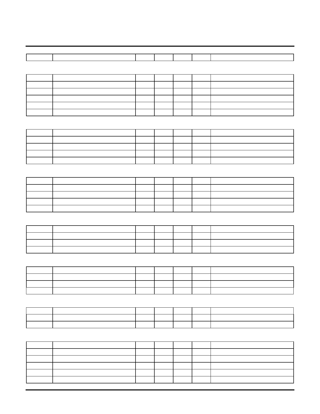
Electrical Characteristics (-40°C TA +85°C unless otherwise noted)
Symbol
Parameter
Min
Typ
Max
Units
HV9606
Conditions
Pre-Regulator/Start-up
VIN
Regulator input voltage
IIN
Input leakage current
IIN
Input leakage current
VDD(REG)
Regulator output voltage
UVLOVDD VDD Under voltage lockout threshold
UVLOVDD VDD Under voltage lockout hysteresis
15
250
V
6
µA VIN 20V, Start = 0V, Stop = 0V
50
µA VIN = 250V
2.8
2.9
3.0
V Vin < 120V
2.7
2.8
2.9
V VDD rising
100
200
mV
Supply (Test Condition: 0.1µF CA to CB and 0.1µF VX2 to PGND)
VDD
Operating range
2.9
5.5
V
IDD
Supply current
1.0
1.5
mA GATE open, fOSC = 50 kHz, VDD = 3.3V
VVX2
Gate drive charge pump supply
1.8xVDD
V
UVLOVX2 VX2 Under voltage lockout threshold
4.5
V
UVLOVX2 VX2 Under voltage lockout hysteresis
0.4
V
Start/Stop Control
VSTART
Start threshold
VSTOP(MAX)
Maximum voltage
VSTOP
Stop threshold
ISTART
Start input current
ISTOP
Stop input current
6.44 7.00 7.56
13
6.44 7.00 7.56
50
50
V VIN rising
V
V VIN falling, VSTART = 0V
nA 6.44V VSTART 7.56V, VSTOP is open
nA 6.44 VSTOP 7.56V, VSTART to 10V via 10k
MOSFET Driver Output (Test condition: VVX2 = 5V)
VGATE(HIGH) Output high voltage
VVX2-0.2
VGATE(LOW) Output low voltage
tR
Rise time
30
tF
Fall time
30
0.15
50
50
V
V
nSec
nSec
IGATE = 10mA
IGATE = -10mA
CLOAD = 250pF
CLOAD = 250pF
Oscillator
fOSC
Initial accuracy
fOSCRANGE
Oscillator Frequency Range
TC
Temperature coefficient
∆f/f
Voltage stability
10
%
30
800
kHz
100
300 PPM/ºC fOSC = 100 kHz
1
2
% fOSC = 100 kHz, 2.9V VDD 5.5V
SYNC
IOSYNC
IISYNC
IVSYNC
Sync output current
Sync input current
Sync input voltage absolute limits
10
20
µA
10
mA VSYNC < 0.1 Volt
-0.5
VDD+0.5
V
PWM
FPWM
PWM Oscillation Frequency
15
400
kHz FPWM = fOSC/2, Stability as fOSC above
DMAX
Maximum duty cycle
49.99
% fOSC = 30kHz
DMAX
Maximum duty cycle
49
% fOSC = 800kHz
DMIN
Minimum pulse width before pulse drop out
130
195
nSec VDD = 3.3V
DMIN
Minimum duty cycle
0
% VFB > VNI, VSS > 2V
DMIN
Minimum duty cycle
0
% VFB < VNI, VSS < 0.1V
2
4/15/2002-R.L2
Supertex, Inc. 1235 Bordeaux Drive, Sunnyvale, CA 94089 TEL: (408) 744-0100 FAX: (408) 222-4895 www.supertex.com
Share Link: 