HV9606X データシートの表示(PDF) - Supertex Inc
部品番号
コンポーネント説明
メーカー
HV9606X Datasheet PDF : 9 Pages
| |||
Absolute Maximum Ratings*
V Input Voltage
-0.3V to +250V
Supply Voltage, VDD
Gate Drive Supply Voltage, VX2
-0.3V to +6V
-0.3 to +15V
Operating Ambient Temperature Range -40°C to +85°C
Storage Temperature Range
-65°C to +150°C
Power Dissipation @ 25°C, SSOP
750mW
Power Dissipation @ 25°C, Plastic DIP
750mW
*All voltages referenced to SGND and PGND pins.
Ordering Information
Package Options
20-Pin SSOP
Dice
HV9606SP
HV9606X
HV9606
__________________________________________________________________________________________________________________
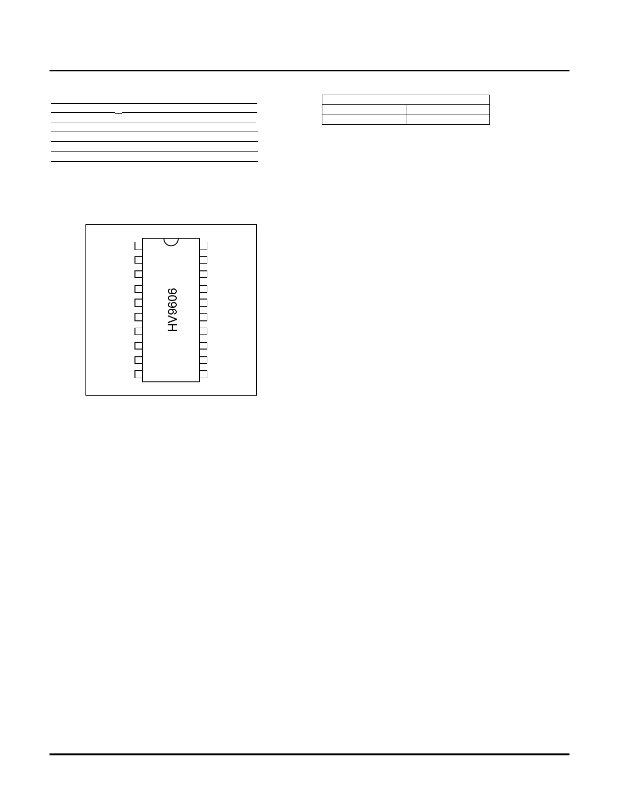
Pinout
SYNC – This I/O pin may be connected to the SYNC pin of other
HV9606 circuits and will cause the oscillators to lock to the highest
frequency oscillator. Synchronization to a master clock is possible
VDD 1
20 STATUS
by means of an open collector or open drain logic gate or
optocoupler, provided the low duty cycle does not exceed 50%. If
START 2
STOP 3
19 SENSE
18 FB
synchronization is utilized then a pull up resistor to VDD is required
to overcome the effects of parasitic capacitance on the circuit
board. The value of the resistor required will depend on the
Vin 4
17 COMP
operating frequency and master clock duty cycle.
REF 5
SS 6
SYNC 7
RT 8
SGND 9
PGND 10
16 NI
15 CA
14 CB
13 VX2
12 GATE
11 CS
RT – The resistor connected from this pin to SGND sets the
frequency of the internal oscillator by setting the charging current
for the internal timing capacitor. The PWM output frequency is one
half the oscillator frequency.
SGND – Common connection for all Logic and Analog circuits.
PGND – Common connection for Gate Driver circuit.
Pin Description
VDD – This is the supply pin for the PWM Logic and Analog circuits.
When the input voltage to the VIN pin exceeds the start voltage the
input regulator seeks to regulate the voltage on the capacitor
connected to this pin to a nominal 2.9V. After the PWM has
started, the bootstrap supply will regulate this voltage to a nominal
3.3V or 5V. With VIN connected to PGND the circuit can be
powered via this pin in the voltage range of 2.9V to 5.5V with a
nominal 2.8V UVLO.
START – The resistive divider from VIN sets the start-up regulator
start voltage.
CS – This is the current sense input. Under normal operation the
over current limit is triggered when the voltage on this pin exceeds
0.5VREF, however, current sensing is blanked during the first 85ns
on time of the MOSFET to prevent false triggering during the turn
on switching transition. The loop control operating peak current
sense may be set to any level below 0.5VREF.
GATE – This push-pull CMOS output is designed to drive the gate
of an N-Channel power MOSFET.
VX2 – This is the supply pin for the Gate Driver circuit and is
generated by the Charge Pump VDD voltage doubler circuit. It
should be bypassed to PGND with a capacitor, typically 0.1µF.
CA and CB – The charge pump circuit uses a capacitor (typically
0.01µF) connected between these pins to generate the VX2
voltage.
STOP – The resistive divider from VIN sets the start-up regulator
stop voltage. A low power sleep mode function may be
implemented by pulling this pin to SGND.
NI – High impedance non-inverting input of the error amplifier.
COMP – The output of the error amplifier.
VIN – This is the startup linear regulator input. It can accept DC
input voltages in the range of 15V to 250V. With START and
STOP programmed to more than 20V, the leakage current on this
pin is less than 6µA at VIN = 20V.
VREF – This pin provides a !1% tolerance reference voltage.
FB – High impedance inverting input of the error amplifier.
SENSE – This is the input pin to the supervisory circuit. On a
rising input voltage the circuit changes state at a nominal 0.85VREF
+ 0.075V. When the input voltage is decaying the circuit changes
state a nominal 0.85VREF – 0.075V.
SS – A capacitor connected to this pin determines the soft start
time. Soft start may be initiated by a low VX2 voltage or an over
current condition when supervisor circuit STATUS output is low.
During short duration input interruptions when the output voltage
does not decay below programmed limits, the supervisor circuit
inhibits soft start to permit rapid recovery of the system.
STATUS – This is the output of the supervisory circuit. When the
sense-input voltage is high, this output is pulled up to VDD by a
10µA current source and the Soft Start function is disabled. When
the sense-input is low, this output is pulled low and it may be used
to directly control the reset of a microprocessor or it may be used
to drive an optocoupler or LED indicator.
4
4/15/2002-R.L2
Supertex, Inc. 1235 Bordeaux Drive, Sunnyvale, CA 94089 TEL: (408) 744-0100 FAX: (408) 222-4895 www.supertex.com
Share Link: 