HV9605 データシートの表示(PDF) - Supertex Inc
部品番号
コンポーネント説明
メーカー
HV9605 Datasheet PDF : 5 Pages
| |||
Pin Description
SGND - Common connection for all low level signal and digital
circuits. While SGND and PGND must be electrically connected
together, having separate common pins enhances the ability of
the designer to prevent coupling of noise into critical circuits.
PGND - This pin provides common return for the high transient
current of the output driver circuits. While PGND and SGND must
be electrically connected, having a separate connection prevents
common noise created by the high transient currents of the output
driver from being injected into critical circuits.
+VIN - This is the start-up linear pre-regulator input which can
accept DC input voltages in the range of 15V to 250V. With
START and STOP set to more than 20V, the leakage current on
this pin is less than 6.0µA at +VIN = 20V.
START - The resistive divider from +VIN sets the start voltage.
STOP - The resistive divider from +VIN sets the stop voltage.
VDD - This is the supply pin for the PWM circuits. When the
input voltage to the +VIN pin exceeds the start voltage the input
regulator seeks to regulate the voltage on the capacitor con-
nected to this pin to a nominal 4.5V.
OUT - This high current push-pull CMOS output is intended
to drive the gate of a power MOSFET. In order to protect the
power MOSFET in high electrical noise environment, this output
appears as low impedance to PGND when VDD is at zero volts.
CS - This is the current sense input to the PWM compara-
tors. Under normal operation the over current limit is triggered
when the voltage on this pin is at 0.70V and the loop control
operating peak current may be set to any level below this, typically
in the range of 0.2 to 0.5V.
HV9605
COMP - The low impedance output of the error amplifier.
FB - The high impedance inverting input of the error amplifier.
NI
- The high impedance non-inverting input of the error
amplifier.
REF - This pin provides a 2% accuracy 1.20V low output
impedance buffered reference which is current limited to 0.5mAmps
and should be bypassed, REF to SGND, with a 0.1µF ceramic
capacitor.
RT - The resistor connected from this pin to SGND sets the
frequency of the internal oscillator by setting the charging current
for the internal timing capacitor. The oscillator frequency is twice
the PWM output frequency.
STATUS - This output is held low until the +VIN voltage reaches
the programmed START voltage. It remains low until the boot-
strap supply to VDD forces the voltage above the internal regulator
set point. It is further held low while the control amplifier output on
the COMP pin is forced to its high limit by a low output from the
converter. Once all these conditions are satisfied, this output will
rise to VDD with a time constant set by the external capacitor
indicating that normal operation has been reached. This output
may be used to control the reset of a microprocessor.
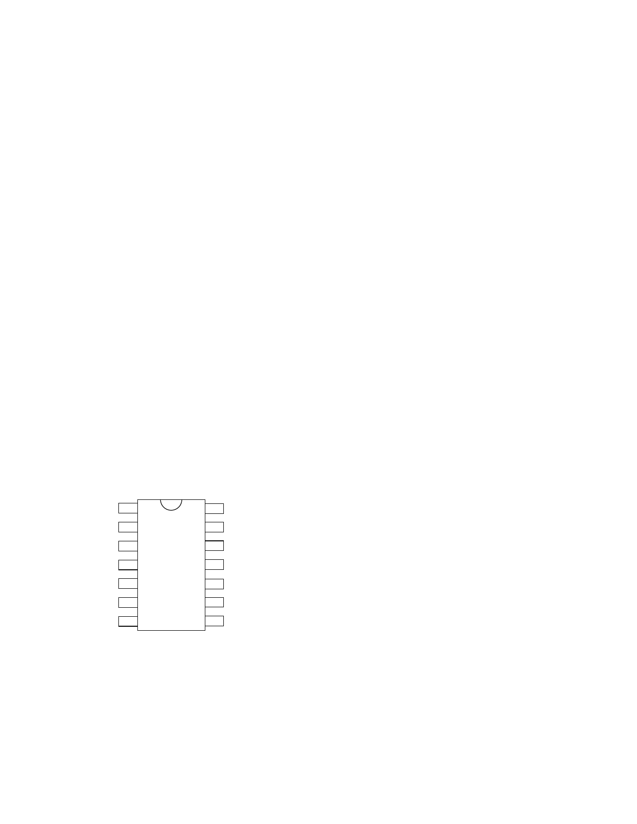
Pin Configuration
+VIN 1
STOP 2
START 3
REF 4
VDD 5
PGND 6
CS 7
14 COMP
13 FB
12 NI
11 STATUS
10 RT
9 SGND
8 OUT
14 Pin SOIC/DIP Package
11/30/98
4
Share Link: 