AH103A гГЗгГЉгВњгВЈгГЉгГИгБЃи°®з§ЇпЉИPDFпЉЙ - WJ Communications => Triquint
йГ®еУБзХ™еПЈ
гВ≥гГ≥гГЭгГЉгГНгГ≥гГИи™ђжШО
гГ°гГЉгВЂгГЉ
AH103A Datasheet PDF : 6 Pages
| |||
AH103A
High Gain, High Linearity ¬љ-Watt Amplifier
The Communications Edge TM
Product Information
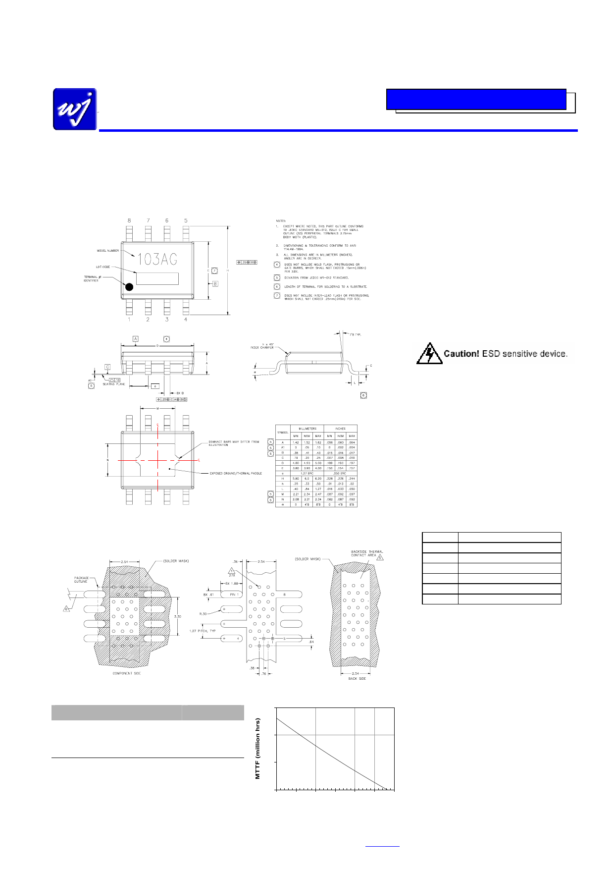
AH103A-G (Lead-Free Package) Mechanical Information
This package is lead-free/green/RoHS-compliant. The plating material on the leads is NiPdAu. It is compatible with both lead-free
(maximum 260°C reflow temperature) and lead (maximum 245°C reflow temperature) soldering processes.
Outline Drawing
Product Marking
The component will be marked with an
вАЬ103AGвАЭ designator followed by a alpha-
numeric lot code on the top surface of the
package.
Tape and reel specifications for this part are
located on the website in the вАЬApplication
NotesвАЭ section.
ESD / MSL Information
ESD Rating:
Value:
Test:
Standard:
Class 1B
Passes 500 V to <1000 V
Human Body Model (HBM)
JEDEC Standard JESD22-A114
ESD Rating:
Value:
Test:
Standard:
Class III
Passes 500 V to <1000 V
Charged Device Model (CDM)
JEDEC Standard JESD22-C101
MSL Rating: Level 2 at +260 °C convection reflow
Standard:
JEDEC Standard J-STD-020
Functional Pin Layout
Mounting Configuration / Land Pattern
Pin
1
2
3, 5, 8
4
6
7
Function
Amp2 input
Amp1 output / Bias Amp1
Ground
RF input (Amp1 input)
RF output (Amp2 output)
Bias Amp2
The backside paddle is the Source and should be
grounded for thermal and electrical purposes. All
other pins should be grounded on the PCB.
Mounting Config. Notes
Thermal Specifications
Parameter
Operating Case Temperature
Thermal Resistance (1), Rth
Junction Temperature (2), Tjc
Rating
-40 to +85° C
20.6° C / W
129° C
1. The thermal resistance is referenced from the hottest part of the junction to
the ground paddle underneath the device.
2. This corresponds to the typical biasing condition of +4.5V, 75mA on pin 1
and 9V, 200 mA on pins 6, 7 at an 85° C case temperature. A minimum
MTTF of 1 million hours is achieved for junction temperatures below 160° C.
MTTF vs. GND Tab Temperature
1000
100
10
1
60 70 80 90 100 110 120
Tab Temperature (°C)
1. Ground / thermal vias are critical for the proper performance
of this device. Vias should use a .35mm (#80 / .0135вАЭ)
diameter drill and have a final plated thru diameter of .25
mm (.010вАЭ).
2. Add as much copper as possible to inner and outer layers
near the part to ensure optimal thermal performance.
3. To ensure reliable operation, device ground paddle-to-
ground pad solder joint is critical.
4. Add mounting screws near the part to fasten the board to a
heatsink. Ensure that the ground / thermal via region
contacts the heatsink.
5. For optimal thermal performance, expose soldermask on
backside where it contacts the heatsink.
6. RF trace width depends upon the PC board material and
construction.
7. Use 1 oz. Copper minimum.
8. All dimensions are in millimeters. Angles are in degrees.
9. A heatsink underneath the area of the PCB for the mounted
device is strictly required for proper thermal operation.
Damage to the device can occur without the use of one.
Specifications and information are subject to change without notice
WJ Communications, Inc вАҐ Phone 1-800-WJ1-4401 вАҐ FAX: 408-577-6621 вАҐ e-mail: sales@wj.com вАҐ Web site: www.wj.com
Page 6 of 6 March 2005
Share Link: 