AIC1577 データシートの表示(PDF) - Analog Intergrations
部品番号
コンポーネント説明
メーカー
AIC1577 Datasheet PDF : 14 Pages
| |||
AIC1577
return to its designed value when the peak inductor
value no longer exceeds over current protection
point.
Over Voltage Protection
Over voltage protection occurs when the FB pin
voltage (the negative input of error amplifier) ex-
ceeds 0.855V. The over voltage comparator will
force driver to pull low until output over voltage is
removed.
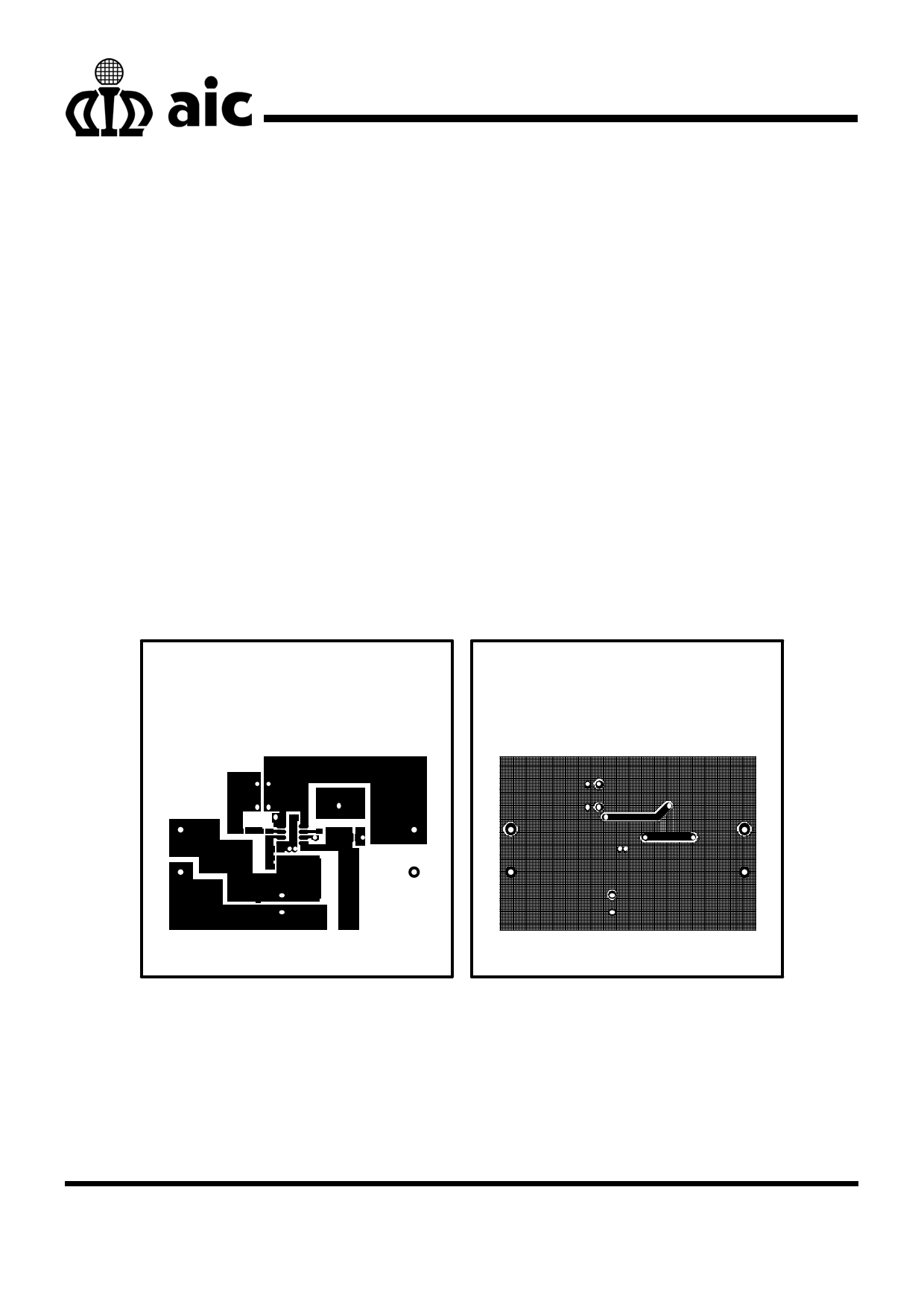
PCB Layout
Since operating in a high switching frequency,
500KHz, proper PCB layout and component place-
ment may enhance the performance of AIC 1577
application circuit. For a better efficiency, major loop
from input terminal to output terminal should be as
short as possible. In addition, in the case of a large
current loop, the track width of each component in
the loop should maintain as wide as possible.
In order to prevent the effect from noise, the GND
pin should be placed close to the ground. Also keep
the IC’s GND pin and the ground leads in the short-
est distance. Recommended layout diagrams and
component placement are as shown as figures 13
to 16. No sensitive components, which may cause
noise interference to the circuit, should be allowed
to be close to SW pin.
Furthermore, AIC1577 is a current mode controller.
Remaining the sense resistor close to both VIN and
CS pins is recommended for better efficiency and
output performance. In addition, all filtering and de-
coupling capacitors, such as C1 and C2, should
connect to AIC1577 as close as possible.
Fig. 13 Top Layer
Fig. 14 Bottom Layer
11
Share Link: 