M29F002 データシートの表示(PDF) - Advanced Micro Devices
部品番号
コンポーネント説明
メーカー
M29F002 Datasheet PDF : 37 Pages
| |||
PRELIMINARY
Contact an AMD representative to obtain a copy of the
appropriate document.
The device is shipped with all sectors unprotected.
AMD offers the option of programming and protecting
sectors at its factory prior to shipping the device
through AMD’s ExpressFlash™ Service. Contact an
AMD representative for details.
It is possible to determine whether a sector is protected
or unprotected. See “Autoselect Mode” for details.
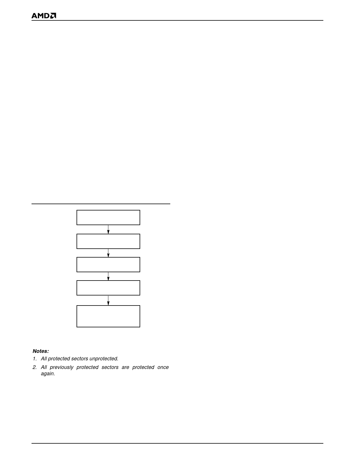
Temporary Sector Unprotect
Note: This feature requites the RESET# pin and is
therefore not available on the Am29F002N.
This feature allows temporary unprotection of previ-
ously protected sectors to change data in-system.
The Sector Unprotect mode is activated by setting the
RESET# pin to VID. During this mode, formerly pro-
tected sectors can be programmed or erased by se-
lecting the sector addresses. Once VID is removed
from the RESET# pin, all the previously protected
sectors are protected again. Figure 1 shows the algo-
rithm, and the Temporary Sector Unprotect diagram
shows the timing waveforms, for this feature.
START
RESET# = VID
(Note 1)
Perform Erase or
Program Operations
Hardware Data Protection
The command sequence requirement of unlock cycles
for programming or erasing provides data protection
against inadvertent writes (refer to the Command Defi-
nitions table). In addition, the following hardware data
protection measures prevent accidental erasure or pro-
gramming, which might otherwise be caused by spuri-
ous system level signals during VCC power-up and
power-down transitions, or from system noise.
Low VCC Write Inhibit
When VCC is less than VLKO, the device does not ac-
cept any write cycles. This protects data during VCC
power-up and power-down. The command register and
all internal program/erase circuits are disabled, and the
device resets. Subsequent writes are ignored until VCC
is greater than VLKO. The system must provide the
proper signals to the control pins to prevent uninten-
tional writes when VCC is greater than VLKO.
Write Pulse “Glitch” Protection
Noise pulses of less than 5 ns (typical) on OE#, CE# or
WE# do not initiate a write cycle.
Logical Inhibit
Write cycles are inhibited by holding any one of OE# =
VIL, CE# = VIH or WE# = VIH. To initiate a write cycle,
CE# and WE# must be a logical zero while OE# is a
logical one.
Power-Up Write Inhibit
If WE# = CE# = VIL and OE# = VIH during power up, the
device does not accept commands on the rising edge
of WE#. The internal state machine is automatically
reset to reading array data on power-up.
RESET# = VIH
Temporary Sector
Unprotect
Completed (Note 2)
Notes:
20818C-4
1. All protected sectors unprotected.
2. All previously protected sectors are protected once
again.
Figure 1. Temporary Sector Unprotect Operation
10
Am29F002/Am29F002N
Share Link: 