AM79C02 データシートの表示(PDF) - Advanced Micro Devices
部品番号
コンポーネント説明
メーカー
AM79C02 Datasheet PDF : 48 Pages
| |||
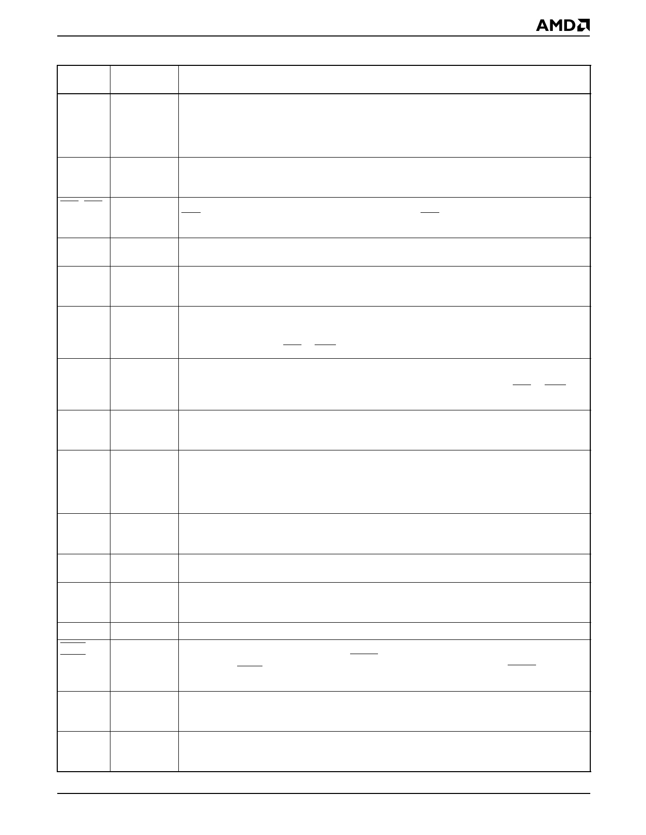
PIN DESCRIPTIONS
Pin
Names
Type
Description
C11–C51,
C12–C52
Inputs/Outputs Control. The five SLIC control lines per channel are TTL compatible and bidirectional. They can
be used to monitor or control the operation of a SLIC or any other device associated with the
subscriber line. Lines C11–C51 are associated with Channel 1, and lines C12–C52 are associated
with Channel 2. The C51 and C52 lines are available on the Am79C02(A) and Am79C031(A). C51
and C52 are output only on the Am79C031(A) and must be programmed as outputs.
CHCLK Output
SLIC Clock. This output provides a 256 kHz or 293 kHz, 50% duty cycle, TTL compatible clock for
use by two SLICs. The CHCLK frequency is derived from MCLK and the phase relationship to
MCLK is random. CHCLK is capable of driving two TTL inputs.
CS2–CS1 Input
Chip Select. The Chip Select inputs (active Low) enable the device to read or write control data.
CS1 is for the Channel 1 microprocessor interface and CS2 is for the Channel 2 microproces-
sor interface.
DCLK
Input
Data Clock. The Data Clock input shifts data into and out of the microprocessor interface of the
DSLAC device. The maximum clock rate is 4.096 MHz.
DIN
Input
Data. Control data is serially written into the Am79C02(A) DSLAC device via the DIN pin with the
most significant bit first. The Data Clock determines the data rate. DIN and DOUT may be strapped
together to reduce the number of connections to the microprocessor.
DIO
Input/Output Data. Control data is serially written into and read out of the Am79C03(A) and Am79C031(A)
DSLAC device via the DIO pin with the most significant bit first. The Data Clock determines the
data rate. DIO is high impedance except when data is being transmitted from these DSLAC
devices under control of CS1 or CS2. DIO replaces DIN and DOUT as found on the Am79C02(A).
DOUT
Output
Data. Control data is serially read out of the Am79C02(A) DSLAC device via the DOUT pin with
the most significant bit first. The Data Clock determines the data rate. DOUT is high impedance
except when data is being transmitted from the DSLAC device under control of CS1 or CS2. DIN
and DOUT may be strapped together to reduce the number of connections to the microprocessor.
DRA, DRB Inputs
PCM. The PCM data for Channels 1 and 2 is serially received on either the DRA or the DRB port
during user programmed time slots. Eight bits are received with the most significant bit first. Data
for each channel is received in 8-bit bursts every 125 µs at the PCLK rate.
DXA, DXB Outputs
PCM. The Transmit PCM data from Channels 1 and 2 is sent serially through either the DXA or
DXB port during user programmed time slots. Eight bits are transmitted with the most significant
bit first. The output is available every 125 µs and the data is shifted out in 8-bit bursts at the PCLK
rate. DXA and DXB are high impedance between bursts and while the device is in the Inactive
mode. DXB is not available on the 79C031(A).
FS
Input
Frame Sync. The Frame Sync pulse is an 8 kHz signal that identifies the beginning of a system’s
PCM frame. The DSLAC device references individual time slots with respect to this input, which
must be synchronized to PCLK.
MCLK
Input
Master Clock. The Master Clock must be a 2.048 MHz or 4.096 MHz clock input for use by the
digital signal processor.
PCLK
Input
PCM Clock. The PCM clock determines the rate at which PCM data is serially shifted into or out
of the PCM ports. PCLK is an integer multiple of the frame sync frequency. The maximum clock
frequency is 8.192 MHz and the minimum clock frequency is 128 kHz.
RST
Input
Reset. A logic Low signal to this pin resets the DSLAC device to its default state. (Am79C02(A) only.)
TSCA,
TSCB
Outputs
Time Slot Control. The Time Slot Control outputs are open drain (requiring pull-up resistors) and
are normally inactive (high impedance). TSCA is active (Low) when PCM data is output on the
DXA pin and TSCB is active (Low) when PCM data is output on the DXB pin. (TSCB is available
on the Am79C02 and Am79C03 only.)
VIN1, VIN2 Inputs
VOUT1,
VOUT2
Outputs
Analog. The analog input is applied to the transmit path of the DSLAC device. The signal is
sampled, digitally processed, and encoded for the PCM output. VIN1 is the input for Channel 1 and
VIN2 is the input for Channel 2.
Analog. The received PCM data is digitally processed and converted to an analog signal at the
VOUT pin. VOUT1 is the output from Channel 1 and VOUT2 is the output for Channel 2. These
outputs can directly drive a transformer SLIC.
SLAC Products
7
Share Link: 