AN3117 データシートの表示(PDF) - Panasonic Corporation
部品番号
コンポーネント説明
メーカー
AN3117 Datasheet PDF : 7 Pages
| |||
AN3117S, AN3117SA
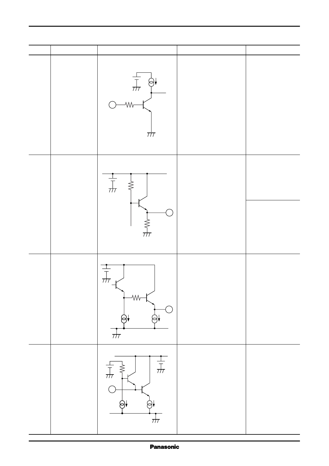
s Terminal Equivalent Circuits (continued)
Pin No. Pin name
Equivalent circuit
13 Antenna switch
10.2 kΩ
13
Other ICs for Video
Description
Standard open voltag
When pin 13 is connected
to VCC, RF oscillator and
driver changeover pin are
operated and when this pin
is open circuited, RF oscilla-
tor is stopped.In this state, no
pop noise will not be made
when antenna switch is
turned on/off even if sound
system is operating.
0.7 V
14 Antenna switch
driver pin
When pin 13 is connected to
Pin 13: VCC
VCC, this pin voltage becomes
4.0 V
4.0 V. (RF oscillator ope- (Load cureent in 15 mA)
2 kΩ
ratesand load current is 15
mA)
When pin 13 is open-cir-
Pin 13: Open
14 cuited, this pin voltage is 0 V.
0V
8 kΩ
(RF oscillator stops)
Drive capability of driver pin
is approx. 30 mA.
15 RF output pin
Output pin of RF signal.
It has low impedance output.
2.7 V
660 Ω
15
16 Video input pin
16
6
The sync. peak value clamp
system is adopted for input
clamp circuit. This pin has a
high input impedance to
minimize sync. distortion.
Pay attention to the sync. sag
which is likely to occur when
an external capacitor attached
is 0.47 µF or less.
2.0 V
Share Link: 