AN211A データシートの表示(PDF) - Motorola => Freescale
部品番号
コンポーネント説明
メーカー
AN211A Datasheet PDF : 12 Pages
| |||
AN211A
Freescale Semiconductor, Inc.
Due to the difficulty of diffusing impurities into both sides
of a semiconductor wafer, a single ended geometry is
normally used instead of the two-sided structure discussed
above. Diffusion for this geometry (Figure 3) is from one side
only. The substrate is of p-type material onto which an n-type
channel is grown epitaxially. A p-type gate is then diffused
into the n-type epitaxial channel. Contact metallization
completes the structure.
The substrate, which functions as Gate 2 of Figure 1, is
of relatively low resistivity material to maximize gain. For the
same purpose, Gate 1 is of very low resistivity material,
allowing the depletion region to spread mostly into the n-type
channel. In most cases the gates are internally connected
together. A tetrode device can be realized by not making
this internal connection.
DRAIN
DRAIN
TYPE C
GATE
SOURCE
GATE
SUBSTRATE
SOURCE
SUBSTRATE
DRAIN
DRAIN
absence of gate voltage is extremely low because the
structure is analogous to two diodes connected back to back.
The metal area of the gate forms a capacitor with the
insulating layers and the semiconductor channel. The metal
area is the top plate; the substrate material and channel are
the bottom plate.
For the structure of Figure 4, consider a positive gate
potential (see Figure 5). Positive charges at the metal side
of the metal-oxide capacitor induce a corresponding negative
charge at the semiconductor side. As the positive charge
at the gate is increased, the negative charge “induced” in
the semiconductor increases until the region beneath the
oxide effectively becomes an n-type semiconductor region,
and current can flow between drain and source through the
“induced” channel. In other words, drain current flow is
“enhanced” by the gate potential. Thus drain current flow can
be modulated by the gate voltage; i.e. the channel resistance
is directly related to the gate voltage. The n-channel structure
may be changed to a p-channel device by reversing the
material types.
DRAIN
GATE
SOURCE
SOURCE
TYPE B
GATE
SOURCE
GATE
SUBSTRATE
SOURCE
SUBSTRATE
NĆCHANNEL MOSFET
PĆCHANNEL MOSFET
MOS FIELD-EFFECT TRANSISTORS (MOSFET)
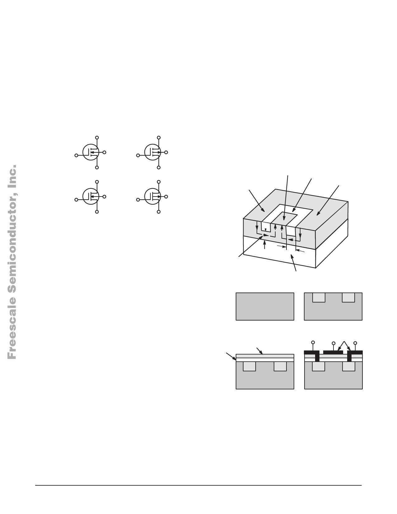
The metal-oxide-semiconductor (MOSFET) operates with
a slightly different control mechanism than the JFET. Figure
4 shows the development. The substrate may be high
resistivity p-type material, as for the 2N4351. This time two
separate low-resistivity n-type regions (source and drain) are
diffused into the substrate as shown in Figure 4b. Next, the
surface of the structure is covered with an insulating oxide
layer and a nitride layer. The oxide layer serves as a
protective coating for the FET surface and to insulate the
channel from the gate. However the oxide is subject to
contamination by sodium ions which are found in varying
quantities in all environments. Such contamination results
in long term instability and changes in device characteristics.
Silicon nitride is impervious to sodium ions and thus is used
to shield the oxide layer from contamination. Holes are cut
into the oxide and nitride layers allowing metallic contact to
the source and drain. Then, the gate metal area is overlaid
on the insulation, covering the entire channel region and,
simultaneously, metal contacts to the drain and source are
made as shown in Figure 4d. The contact to the metal area
covering the channel is the gate terminal. Note that there
is no physical penetration of the metal through the oxide and
nitride into the substrate. Since the drain and source are
isolated by the substrate, any drain-to-source current in the
CHANNËËËËEL ËËËË(SËËËËUBPSËËËËTRPAITNDËËËËE) ËËËËPL ËËËËËËËËËËËËËËËËËËËËËËËËËËËË
CHANNEL LENGTH
Figure 3. Junction FET with Single-Ended Geometry
SOURCE
DRAIN
P
(SUBSTRATE)
N
N
P
(SUBSTRATE)
(a)
(b)
SILICON NITRATE
OXIDE
SiO2
Si3N4
ÉÉÉÉÉÉÉÉÉÉÉÉÉÉÉÉÉÉÉÉÉÉÉÉÉÉÉÉ N
N
S
G METAL D
N
N
P
P
(SUBSTRATE)
(SUBSTRATE)
(c)
(d)
Figure 4. Development of Enhancement-Mode
N-Channel MOSFET
2
For More InformMaOtiToOnROOLnATShEiMsICPOrNoDdUuCcTtO, R APPLICATION INFORMATION
Go to: www.freescale.com
Share Link: 