AN606 データシートの表示(PDF) - Vishay Semiconductors
部品番号
コンポーネント説明
メーカー
AN606 Datasheet PDF : 4 Pages
| |||
AN606
Vishay Siliconix
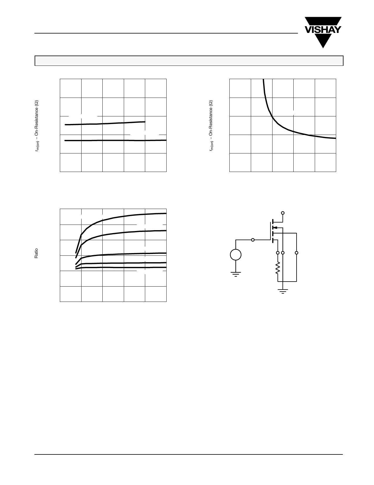
TYPICAL CHARACTERISTICS (25_C UNLESS NOTED)
On-Resistance vs. Sense Current
10
10
SENSE DIE
On-Resistance vs. Gate-Source Voltage
8
6
VGS = 4.5 V
4
VGS = 10 V
8
6
ID = 10 mA
4
2
2
0
0.00
1200
1000
800
600
400
200
0.02
0.04
0.06
0.08
0.10
ISENSE (A)
Current Ratio (I(MAIN)/IS)
vs. Gate-Source Voltage (Figure 1)
RS = 6.6 W
RS = 4.7 W
RS = 2.2 W
RS = 1.1 W
RS = 0.5 W
0
0
2
4
6
8
10
VGS − Gate-to-Source Voltage (V)
G
SENSE
VG
RS
S KELVIN
0
0
4
8
12
16
20
VGS − Gate-to-Source Voltage (V)
FIGURE 2. Current-Sensing Die Characteristics and Schematic
Definition of Current-Sensing Parameters
The current-sense ratio, r, is the quotient of the number of cells
terminated on the sense terminal to the total number of cells on
the MOSFET die.
To derive the value of r using the above definition requires
detailed die design. However, the quotient of drain current to
the sense current provides the same value because these
current values are the sum of cell current in each path.
Mathematically:
r = ID/ISENSE
ID is drain current
www.vishay.com
2
ISENSE is the current flowing out of the sense terminal and into
the sense resistor, RSENSE
Mirror active resistance, rm(on), is the resistance of parallel
connected cells used in the sense chain when the device is on.
Being rDS(on) as in any other MOSFET, the value depends on
the gate drive, drain current, and junction temperature.
Accordingly, rm(on) is defined at given values of VGS, IDRAIN,
and TJ junction.
By definition, for the sense die, refer to Figure 2. Mirror active
resistance rm(on) is specified at the gate-source voltages, VGS
at 4.5 V and 10 V, corresponding drain-source current ISENSE
up to 0.1 A, and junction temperature TJ at 25 _C. The
temperature coefficient of rm(on) is the same as that of rDS(on).
Refer to the on-resistance vs. junction temperature curve in
Figure 3.
Document Number: 71991
17-Dec-03
Share Link: 