AN723 データシートの表示(PDF) - Vishay Semiconductors
部品番号
コンポーネント説明
メーカー
AN723 Datasheet PDF : 8 Pages
| |||
AN723
Vishay Siliconix
Start-Up/UVLO
The internal under voltage lock out (UVLO) circuit keeps most
of the IC function blocks off until the supply voltage (VDD)
increases above 2.4 V. A 100-mV hysteresis is built into the
UVLO point, so the controller will be functional until VDD drops
below 2.3 V. This helps to eliminate the IC from bouncing
between ON and OFF stages. After the IC is turned ON, it
takes about 4 ms for the POR to be ready, the error amp
output to charge up, and the output voltage to start ramping
up. The output voltage will need an additional 3 to 4 ms to
reach regulation, depending on load condition.
By-Pass Mode
When using the Si9165, the output voltage regulation point
can be set within the input voltage range, regardless of
whether a buck or boost configuration is being used. For
instance, for an input range of 2.7 V to 4.2 V, the output
voltage could be set to 3.3 V.
For a boost converter, when the input is higher than 3.3 V, the
duty cycle of the switch stays at 0%, and the output voltage
follows the input voltage by a voltage drop consisting of
inductor resistance and MOSFET (in PWM mode) or diode (in
PSM mode) drop. When the input decreases and approaches
3.3 V, the output drops to the regulation point, and the main
switch starts to switch at a minimum duty cycle to keep the
output regulated at 3.3 V. This duty cycle increases as the
input voltage decreases. In some instances, noise can be
generated during the transition because there is a minimum
controllable duty cycle for any PWM controller. The frequency
and amplitude of this transition noise vary depending on the
compensation network. The wider the loop bandwidth (BW),
the higher the switching frequency and the lower the output
ripple.
For a buck converter, when input voltage is higher than 3.3 V,
it is stepped down to 3.3 V at the output. As the input
decreases and approaches 3.3 V, the switching duty cycle
increases to the maximum duty cycle, jumping to 100% and
making the high-side switch work like a saturated linear
regulator. The output voltage will simply follow the input
voltage by the saturation voltage until the input drops below
the UVLO voltage or until another user-defined control signal
disables the converter. The same noise considerations as for
a boost converter apply in this case.
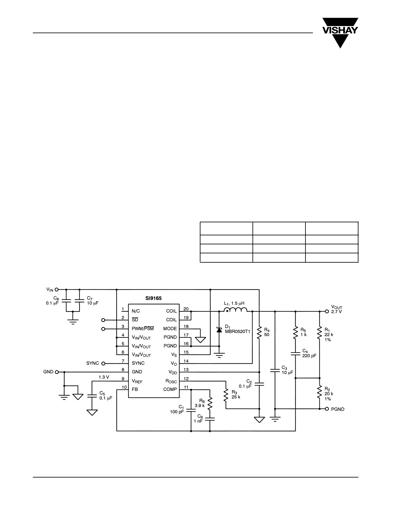
Buck/Boost Configuration
The Si9165 can be easily configured to function as a step-
down (buck) or a step-up (boost) converter. Figures 2 and 3
show the typical application circuit for buck and boost
converters, respectively. The list in Table 1 shows the key IC
connection differences in the two topologies.
TABLE 1. Buck-Boost Pin Connection Comparison
Name of Pin
Buck
Boost
VIN/VOUT
MODE
VS
Input
Low
Input
Output
High
Output
FIGURE 2. Typical Application Circuit-Buck
FaxBack 408-970-5600, request 70823
2
www.siliconix.com
Share Link: 