AN723 データシートの表示(PDF) - Vishay Semiconductors
部品番号
コンポーネント説明
メーカー
AN723 Datasheet PDF : 8 Pages
| |||
AN723
Vishay Siliconix
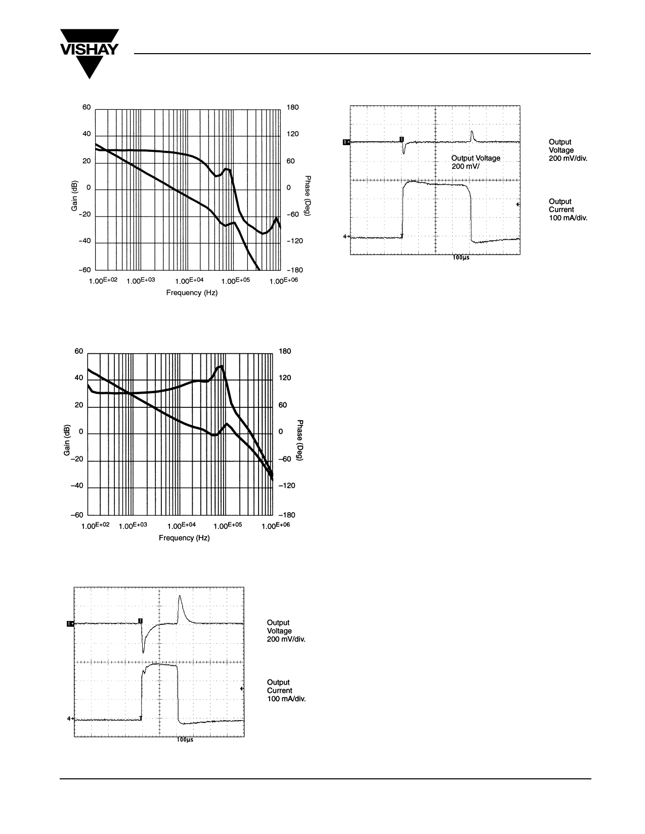
FIGURE 6. Buck Converter Loop Gain with Type I
Compensation
FIGURE 7. Buck Converter Loop Gain with Type III
Compensation
FIGURE 9. Buck Load Transient w/Type III Compensation
VIN = 3.6 V, VOUT = 2.64 V, 300 mA Load Transient
For voltage mode control, a simple Type I or II compensation
network can easily stabilize the loop but at a cost of lower BW,
which has to be at least one decade below the L-C corner
frequency to preserve a good stability margin. However, Type
III compensation, a more complicated design, enables higher
BW even above the L-C double-pole. A buck converter is used
as an example here to illustrate the difference between Type I
(Figure 6) and Type III (Figure 7) compensation. With the
switching frequency set to 2 MHz, a 1.5-µH to 10-µF L-C pair
is used for the power stage, producing a double pole at
40 kHz. The loop gain Bode plots are measured for both types
under the same conditions: VIN = 3.6 V, VOUT = 2.7 V, load =
300 mA. (See Figures 8 and 9). The BW is considerably
higher with Type III compensation. The resulting transient
waveforms for the two loops (Figures 10 and 11) show a
notable improvement in both over/undershoot magnitude and
recovery time with Type III compensation.
The values shown in Figure 7 work well for the Si9165 buck
converter with a 3.6-V input, so long as the switching
frequency is above 500 kHz, which is the range Si9165 is
optimized for. Since the converter power stage gain varies
with input voltage, the compensation circuit needs to be
adjusted accordingly to maintain a stability margin. The
circuitry in Figure 7 offers fast response with a sufficient
stability margin for input voltages below 3.6 V. If the input
voltage is above 3.6 V, the power stage gain, also part of the
loop gain, elevates to a level that will endanger both the phase
margin and gain margin of the control loop. Fortunately for
buck converters, a simple change on the input lead capacitor
C3 can help compensate for this. The value can be adjusted
by the simple equation shown below:
C3
=
3----.-6----V------⋅---2---7---0----p----F--
VIN
(5)
FIGURE 8. Buck Load Transient w/Type I Compensation
VIN = 3.61 V, VOUT = 2.676 V, 300 mA Load Transient
FaxBack 408-970-5600, request 70823
www.siliconix.com
5
Share Link: 