AN701 データシートの表示(PDF) - Vishay Semiconductors
部品番号
コンポーネント説明
メーカー
AN701
Vishay Semiconductors

AN701 Datasheet PDF : 19 Pages
| |||
AN701
Vishay Siliconix
FUNCTIONAL DESCRIPTION OF THE
SI9114A BID/CMOS PWM CONTROLLER
The Si9114A controller is similar in configuration to the Si9110.
It uses a traditional constant frequency current mode control,
the most commonly used architecture. The duty cycle is limited
to less than 50% to avoid problems with core reset.
Current mode control is presently the de-facto standard for
PWM control circuits. Indeed, it is the only candidate that
should be considered, given its many advantages:
S Cycle by cycle current limit protection
S Simple loop compensation, eliminating effect of output
inductor
S Excellent fast transient response due to inner control loop
S Automatic input voltage feed-forward compensation
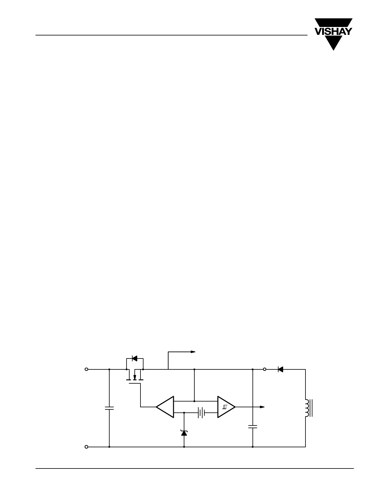
PIN 1 Ć HIGH VOLTAGE PREĆREGULATOR
All switchmode power supplies face a start-up problem caused
by the large difference between dc bus voltage and the VCC
power rail for supplying the control circuit. The traditional
technique has been to keep the control circuit in “sleep mode,”
while a small amount of energy is used to “top up” a large
enough electrolytic capacitor to get the circuit started. When
the circuit starts operating, a winding on the transformer is then
used to power the control circuit. Disadvantages with this type
of circuit include delayed start-up and large required
capacitances for guaranteed operation over the full voltage
range. The Si9114A overcomes these problems by using low
power consumption, BiC/DMOS circuitry, and a unique
high-voltage depletion mode MOSFET. (See 2)
When power is first applied, the depletion transistor is on, and
current flows from the input capacitor CIN into the VCC
capacitor CVCC until VCC reaches 9.2 V. The converter
transformer will then supply the VCC through a bias winding,
which will raise VCC to a level higher than 9.2 V. Ideally this will
be between 11 and 13 V, thus turning off the high-voltage
+VIN
depletion mode MOSFET. The 9.2-V threshold has a
hysteresis of 300 mV to prevent oscillations when the
transition voltage is not clearly defined or when high-line
supply impedance is encountered.
For applications where the input dc voltage is not high, and the
chip power consumption is not excessive, the feedback
winding can be eliminated. In such cases, the pre-regulator
circuit will behave just like a linear regulator with 9.2-V output
and 10-kW series resistance. In this case, the parameters to be
considered are the dropout voltage at lowest line condition and
the power dissipation at highest voltage. The high-voltage
depletion mode MOSFET contains an internal body diode, and
in situations where the VCC is being powered from a laboratory
supply, care must be taken to avoid loading the +VIN rail
beyond the current rating of this device. Typically, the reverse
characteristics of the device will generate a voltage of 3.4 V on
Pin 1 with 10-kW load when powering VCC from a lab supply.
In some applications it is necessary to inhibit the start of a
converter until a high enough voltage is present on the supply
bus. This is the case for the following reasons:
S Circuitry fed from a high line impedance such as a
telephone line will have difficulty starting, since the
converter will behave like a negative impedance. As the dc
voltage decreases, the input current increases because
constant power is drawn. This causes severe oscillations,
and can in some instances have a destructive effect on the
converter. [4]
S During start-up, the Si9114A will begin operation as soon
as the UVLO threshold is reached. Since the converter is
designed to operate over a much higher range—for
example, from 36 to 72 V—then between 10- and 36-V
input the output voltage will be out of regulation and
undefined. In some cases, digital circuitry will not accept
this mode of operation, and system faults will be
encountered without a RESET watchdog circuit.
To overcome these problems, a Zener diode of suitable value
VZ can be placed in series with the +Vin pin, preventing start-up
until VZ + 9.2 V is reached.
To Internal Circuits
VCC
Transformer Winding
CIN
–VIN
www.vishay.com
2
–
+
0.2 V
9.2 V
300 mV
–
UVLO
+
CVCC
Figure 2 Start Circuit
Document Number: 70575
16-Jan-01
Share Link: