AN701 データシートの表示(PDF) - Vishay Semiconductors
部品番号
コンポーネント説明
メーカー
AN701
Vishay Semiconductors

AN701 Datasheet PDF : 19 Pages
| |||
AN701
Vishay Siliconix
I1
C1
VREF
C2
RT
Q1
CT
Q2
B1
B2
I2
U1
DQ
CLK
Q
B3
SYNC
SW1
IC1
1
2
+VIN
SHD
VCC
Sense
14
13
3
4
VREF
NI
5 FB
Out 12
–VIN
SYNC
11
10
6
7
COMP
SS
COSC
ROSC
9
8
Si9114A Rt
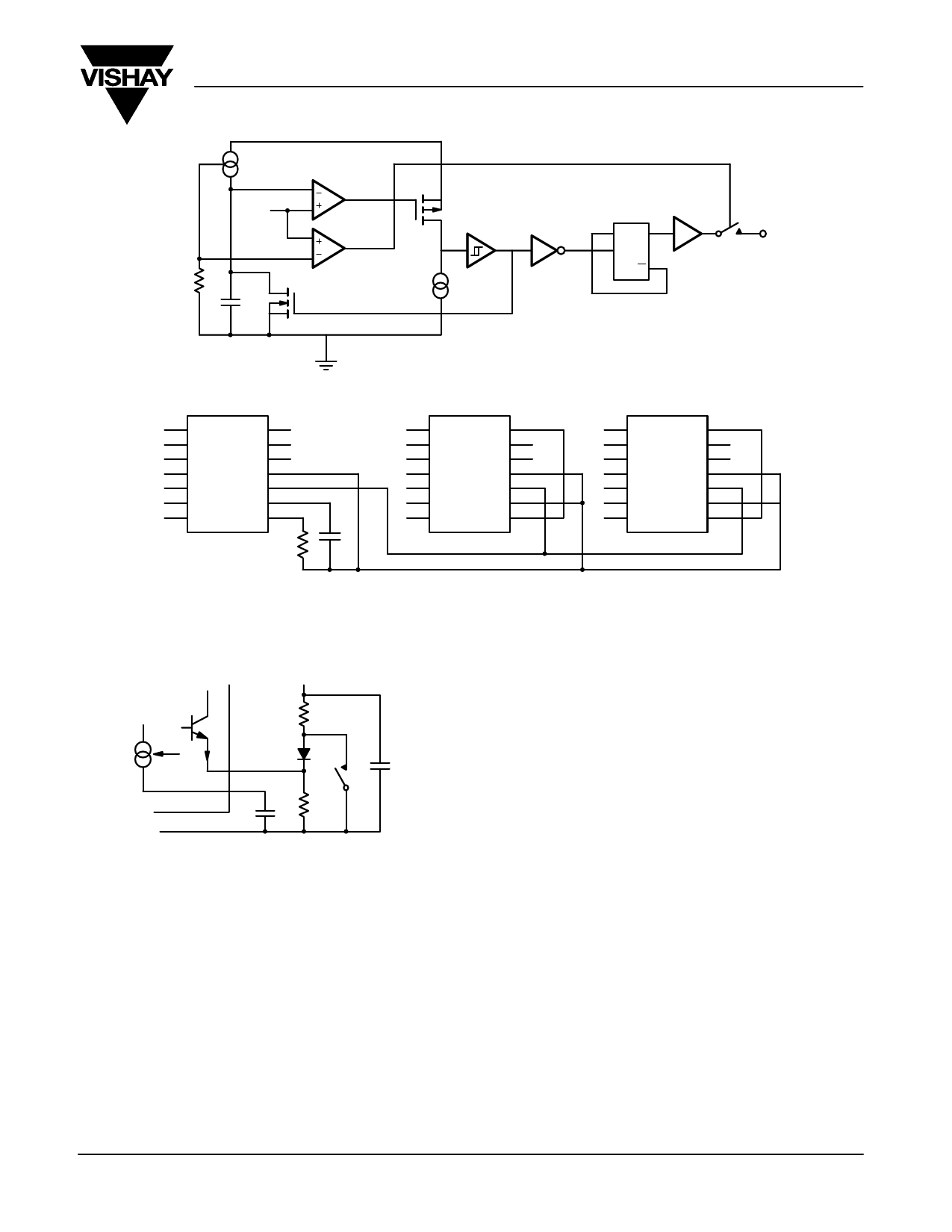
Figure 7 Oscillator
IC2
1
2
+VIN
SHD
VCC
Sense
14
13
3
4
VREF
NI
5 FB
Out 12
–VIN
SYNC
11
10
6
7
COMP
SS
COSC
ROSC
9
8
Ct
Si9114A
IC3
1
2
+VIN
SHD
VCC
Sense
14
13
3
4
VREF
NI
5 FB
Out 12
–VIN
SYNC
11
10
6
7
COMP
SS
COSC
ROSC
9
8
Si9114A
Figure 8 Oscillator Synchronization
VCC
–VIN
R1
120 k
Rt
D1
CVCC
1 mF
Ct
SW1
RT
CT
68 k
SW1 Closed = Frequency High
SW1 Open = Frequency Low
Figure 9 Frequency Shifting Using Rt Current Change
In certain circumstances, such as current limiting, it may be
desirable to change the frequency of the converter for a period
of time to overcome current tails (see Figure 16 for further
explanation). With the Si9114A, this is easily done by adding
or subtracting some current into the RT terminal:
S The charging current in CT is set by 8 RT.
S The voltage at the RT terminal is 4 V, as supplied by an
internal emitter follower from the reference.
The frequency can be changed easily by supplying some of
the current into RT from the VCC rail, thus “starving” the
internal current source, and slowing the frequency down.
Document Number: 70575
16-Jan-01
The current in RT is set by V = IR where V = 4 V and R = RT.
Using a diode, and some type of switch, the frequency can be
easily changed: when SW1 is closed, D1 is reverse biased, and
has no effect on RT. When SW1 is open, current flows through
R1 and D1 into RT and removes some of the current supplied
by the internal emitter follower.
PIN 10 Ć SYNCHRONIZATION
The SYNC input allows operation from a master clock as the
connection is made after the divide-by-two. As a result,
synchronization in both frequency and phase is possible. This
unique feature is important to systems designers who use
multiple converters, where noise caused by an
unsynchronized “beating” effect is present and causes difficult
EMI/EMC problems. If an external clock is used, duty cycles of
>50% are possible due to the position of the SYNC pin , after
the divide-by-two. Where >50% conduction is used, core reset
must be allowed, in order to prevent core saturation.
Synchronization is in master/slave mode, with one device (the
“master”) setting the switching frequency and others (the
“slaves”) with disabled oscillators locked to it. Alternatively, all
devices can be clocked using a master oscillator.
During slave mode, the unused CT pin should be connected to
ground, and the RT to VCC.
www.vishay.com
5
Share Link: