AN701 データシートの表示(PDF) - Vishay Semiconductors
部品番号
コンポーネント説明
メーカー
AN701
Vishay Semiconductors

AN701 Datasheet PDF : 19 Pages
| |||
AN701
Vishay Siliconix
+
Tx1
Si9114ADY
1
14
+Vin
VCC
2
13
SHUTDOWN Sense
3
Vref
12
Output
4
NI
5
6 FB
COMP
11
–Vin
10
SYNC
9
COSC
7
SS
8
ROSC
Rfilt
Cfilt
Cin Cref Css
–
Q1
Rsense
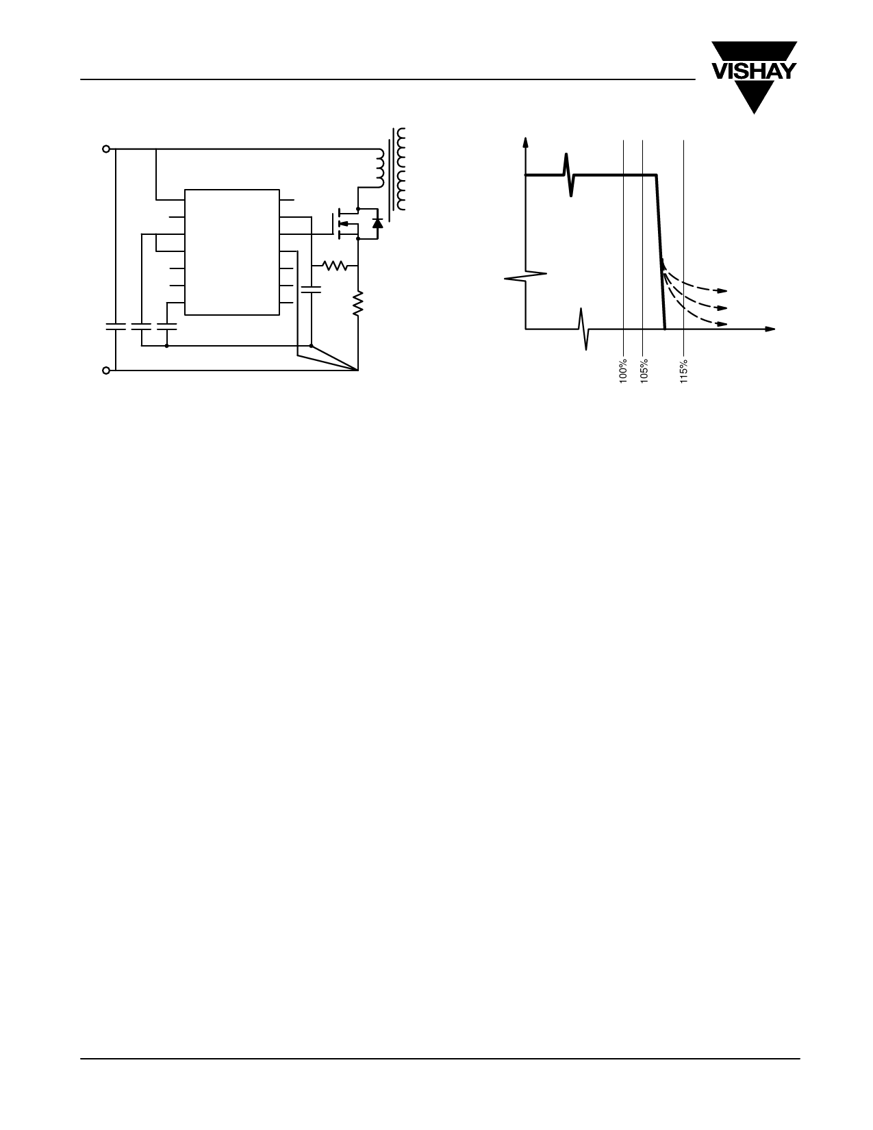
Figure 15
Volts
Current
Tail
Amps
Figure 16
LAYOUT CONSIDERATIONS
The main current loop flows from the input capacitor—through
the transformer, MOSFET, and sense resistor—and returns to
the capacitor. This current will have high rates of change and
associated fast voltage and current edges. It is essential to
avoid the injection of noise into the other circuitry.
To prevent this result, a “fishbone” type arrangement is
recommended (Figure 15). Designers are encouraged to
separate different grounds with “imaginary” dummy resistors.
These can be removed at a later stage. Main current loops
must be designed to be as short as possible: from CIN to the
transformer, through the MOSFET and Sense resistor, and
back into CIN. It is obvious that signals switching 50 V or 1 A
in 25 ns should not be mixed with signals that are controlling
a closed-loop, high-gain feedback system which is capable
of regulating the output voltage to less than 1 mV.
CHOOSING THE SWITCHING FREQUENCY
When selecting the switching frequency, it is usually best to
choose the lowest possible frequency that the design solution
will accept. In PWM control topologies, the maximum switching
frequency will be strongly governed by short circuit behavior.
When a short circuit is applied to the output, the control circuit
is required to reduce the duty cycle to the smallest possible
value to maintain constant current operation (Figure 16).
Ideally, the converter should deliver 105% of the output current
within regulation and no more than 115% under short circuit. At
500 kHz, the period of conversion is 2 ms and the maximum on
time is 1 ms.
High minimum duty ratios will result in current tails and require
rectifier oversizing to avoid destructive currents under
overload conditions.
The Si9114A has a sync-to-output delay of less than 70 ns,
so the minimum duty cycle for operation at 500 kHz would
www.vishay.com
8
be 70 ns/2 ms = 3.5%. This minimum should be considered
when the short circuit current is determined. Designers
should note that a shunt placed across the output of the
converter is probably not a realistic load in the event of a failure,
and the real circuit impedance will probably be substantially
lower. In such circumstances, it may be necessary to shift the
frequency of the converter to a lower value during overload.
Frequency shifting can be accomplished by altering the steady
state values of the oscillator programming components (see
oscillator section, Figure 8).
SHORT CIRCUIT BEHAVIOR
Short circuit behavior is different for both common topologies,
and must be paid special attention.
S In flyback converters, all windings appear in “parallel” with
each other. When one winding is shorted, all other flyback
windings are also shorted though it. In multiple output
converters, therefore, any single winding without a
separate secondary current-limiting protection will “drag
down” all the other windings. As a result, if a bias winding
is used to power the control circuit, it will stop delivering
power. When this occurs, the Si9114A depletion device will
turn on and regulate the supply rail to 9.2 V, as in its normal
starting mode. In this event, designers should calculate the
worst-case power dissipation caused by the voltage drop
across the depletion transistor at the highest applied
voltage across it and with the current flowing through it.
S In forward converters, traditionally the bias winding is also
taken in forward conduction mode, but without any series
inductance. In the event of a short circuit, the pulse width
is reduced to minimum, but it is sufficient to supply enough
power to the control circuit. This is an advantage, and
avoids the problems encountered with flyback converters.
Power may also be taken in flyback mode, however, when
the duty cycle is low. There will be very little flyback voltage
present, since the applied volt/microseconds is low and the
core need not, therefore, fly back very far to reset.
Document Number: 70575
16-Jan-01
Share Link: