AN8014 データシートの表示(PDF) - Panasonic Corporation
部品番号
コンポーネント説明
メーカー
AN8014 Datasheet PDF : 18 Pages
| |||
Voltage regulators
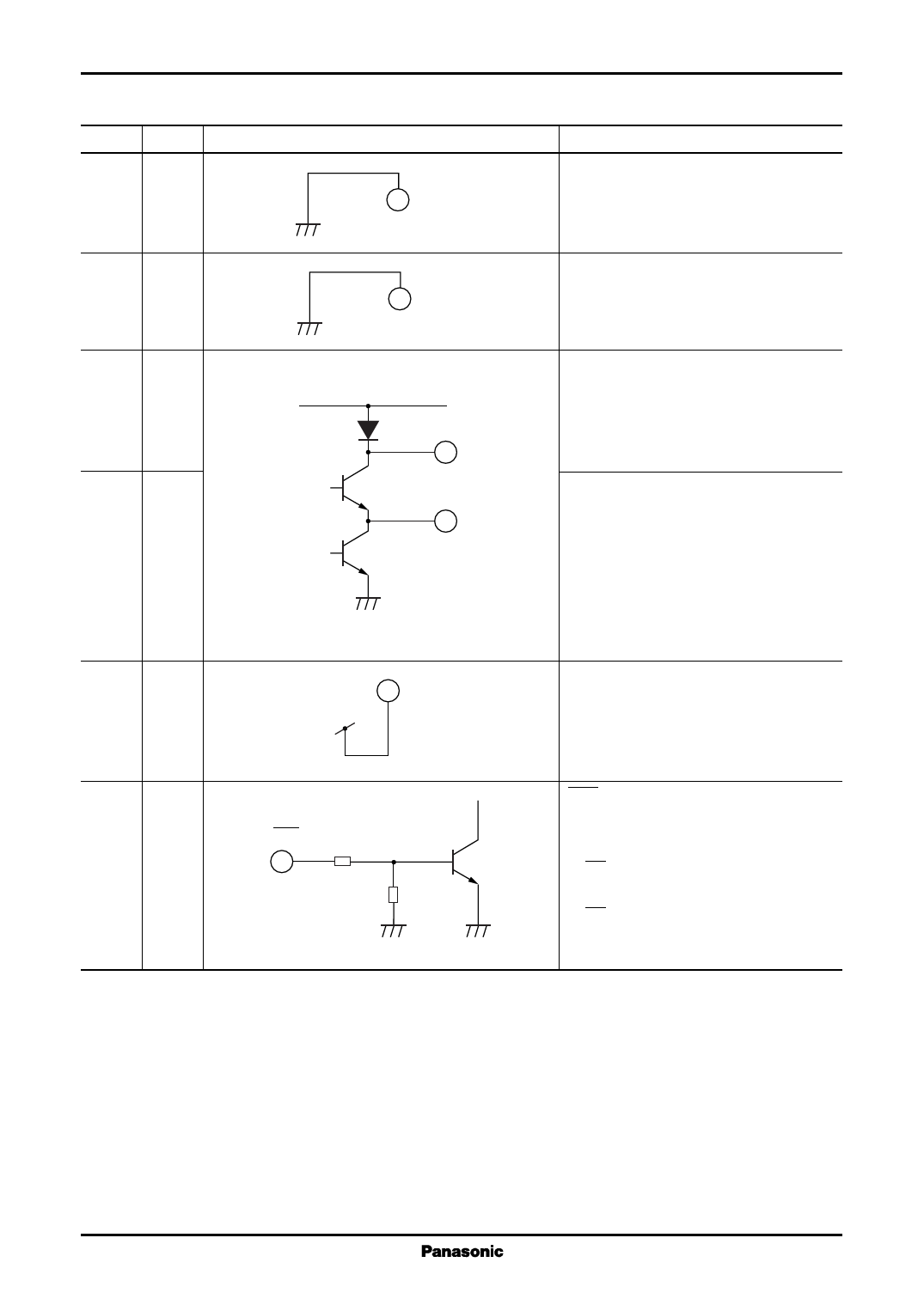
s Terminal Equivalent Circuits (continued)
Pin No. I / O
Equivalent circuit
11
11 SGND
12
12 GND
13
O
VCC
14
O
14 CB
13 Out
15
I
16
I
15
VCC
OFF 17 kΩ
16
13 kΩ
AN8014S
Description
SGND: Signal ground.
GND: Output stage ground.
Out:
Totem pole output.
A constant output current of ±100 mA or a
peak output current of ±1 A can be ob-
tained.
CB:
Bootstrap output.
Connect a bootstrap capacitor between
this pin and the n-channel MOSFET source-
side pin of the switching element when
using a step-down voltage circuit.
Short-circuit this pin and the VCC pin when
using a step-up voltage circuit.
VCC: Power supply.
OFF:
Controls the on/off state.
When the input is high: normal operation
(VOFF > 2.0 V)
When the input is low: standby mode
(VOFF < 0.8 V)
In standby mode, the total current consu-
mption is held to under 10 µA.
s Application Notes
[1] Function descriptions
1. Reference voltage block
This block is composed of the band gap circuit and outputs the temperature compensated reference voltage (2.6
V) to the VREF pin (pin 1). The reference voltage is stabilized when the supply voltage is 3.6 V or more and used
as the operating power supply in IC. It is possible to take out a load current of up to −1 mA.
7
Share Link: 