AP1522 データシートの表示(PDF) - Anachip Corporation
部品番号
コンポーネント説明
メーカー
AP1522 Datasheet PDF : 8 Pages
| |||
Step-Up DC/DC Converter
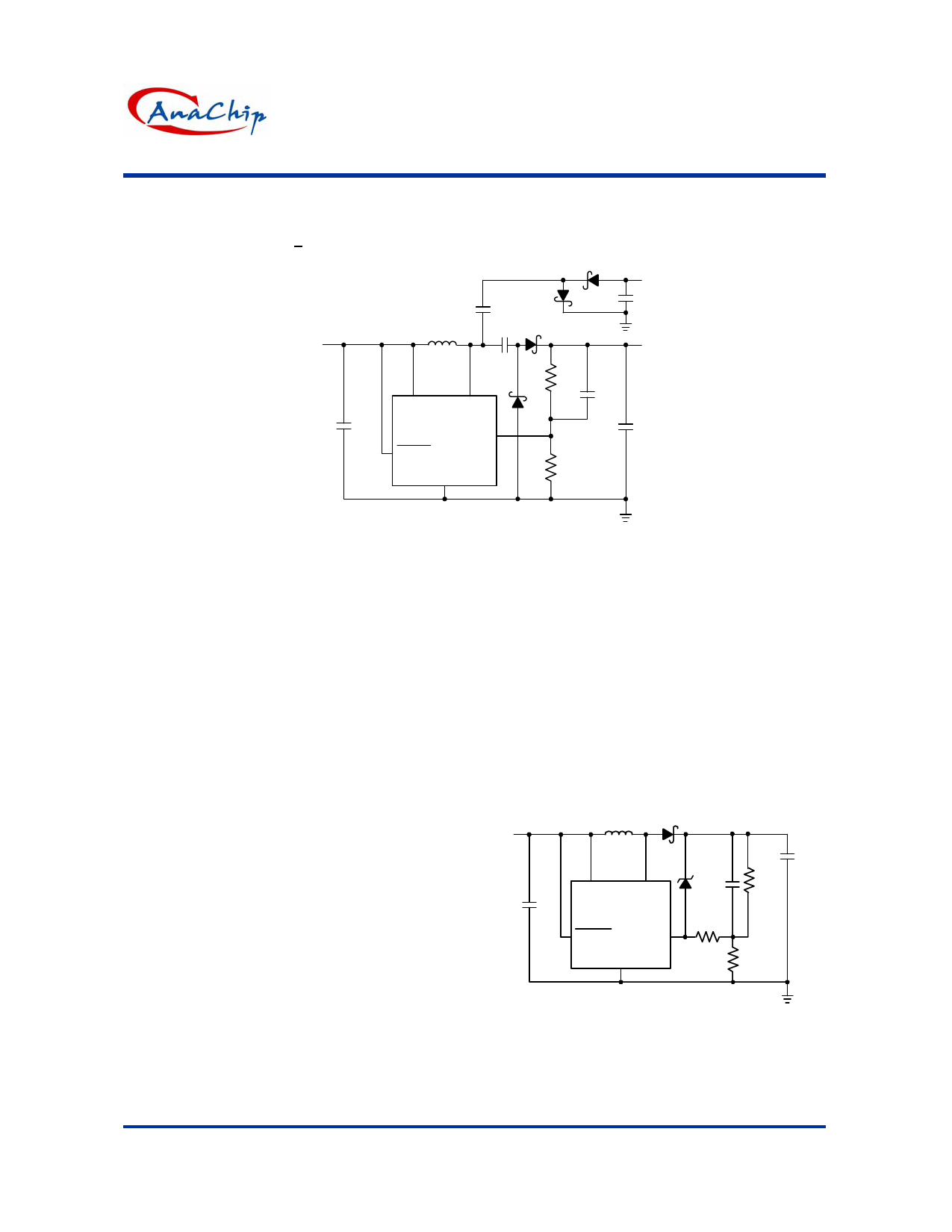
Typical Application Circuit (Continued)
+20V Dual Output Converter with Output Disconnect
VIN
2.5V to 5V
D3
-20V
C4
1uF
L1
10uH
D2
C5
1uF D1
4mA
C3
1uF
20V
4mA
5
1
D4
C1
4.7uF
VIN
SW
AP1522 FB 3
4 SHDN
GND
2
150K 4.7pF
10K
C2
10uF
AP1522
Applications Information
Inductor Selection
A 10µH inductor is recommended for most AP1522
applications. Although small size and high
efficiency are major concerns, the inductor should
have low core losses at 1MHz and low DCR
(copper wire resistance).
Capacitor Selection
The small size of ceramic capacitors makes them
ideal for AP1522 applications. X5R and X7R types
are recommended because they retain their
capacitance over wider voltage and temperature
ranges than other types such as Y5V or Z5U. A
4.7µF input capacitor and a 4.7µF output capacitor
are sufficient for most AP1522 applications.
Diode Selection
Schottky diodes, with their low forward voltage drop
and fast reverse recovery, are the ideal choices for
AP1522 applications. The forward voltage drop of
a Schottky diode represents the conduction losses
in the diode, while the diode capacitance (CT or CD)
represents the switching losses. For diode
selection, both forward voltage drop and diode
capacitance need to be considered. Schottky
diodes with higher current ratings usually have
lower forward voltage drop and larger diode
capacitance, which can cause significant switching
losses at the 1MHz switching frequency of the
AP1522. A Schottky diode rated at 100mA to
200mA is sufficient for most AP1522 applications.
Open-Circuit Protection
In the cases of output open circuit, when the R1 are
disconnected from the circuit, the feedback voltage
will be zero. The AP1522 will then switch at a high
duty cycle resulting in a high output voltage, which
may cause the SW pin voltage to exceed its
maximum 36V rating. A zener diode can be used
at the output to limit the voltage on the SW pin
(Figure 1). The zener voltage should be larger
than the maximum forward voltage of the VOUT.
The current rating of the zener should be larger
than 0.1mA.
V IN
L
22uH
D
COUT
2uF
VIN
SW
CIN
1uF
AP1522
SHDN
FB
4.7pF
R2
1K
R1
200K
R3
GND
14K
Figure 1. With Open-Circuit Protection
Anachip Corp.
www.anachip.com.tw
Rev. 1.0 May. 5, 2005
5/8
Share Link: 