AP2129K-ADJTRG1(2008) データシートの表示(PDF) - BCD Semiconductor
部品番号
コンポーネント説明
メーカー
AP2129K-ADJTRG1 Datasheet PDF : 15 Pages
| |||
Data Sheet
300mA HIGH SPEED, EXTREMELY LOW NOISE CMOS LDO REGULATOR
AP2129
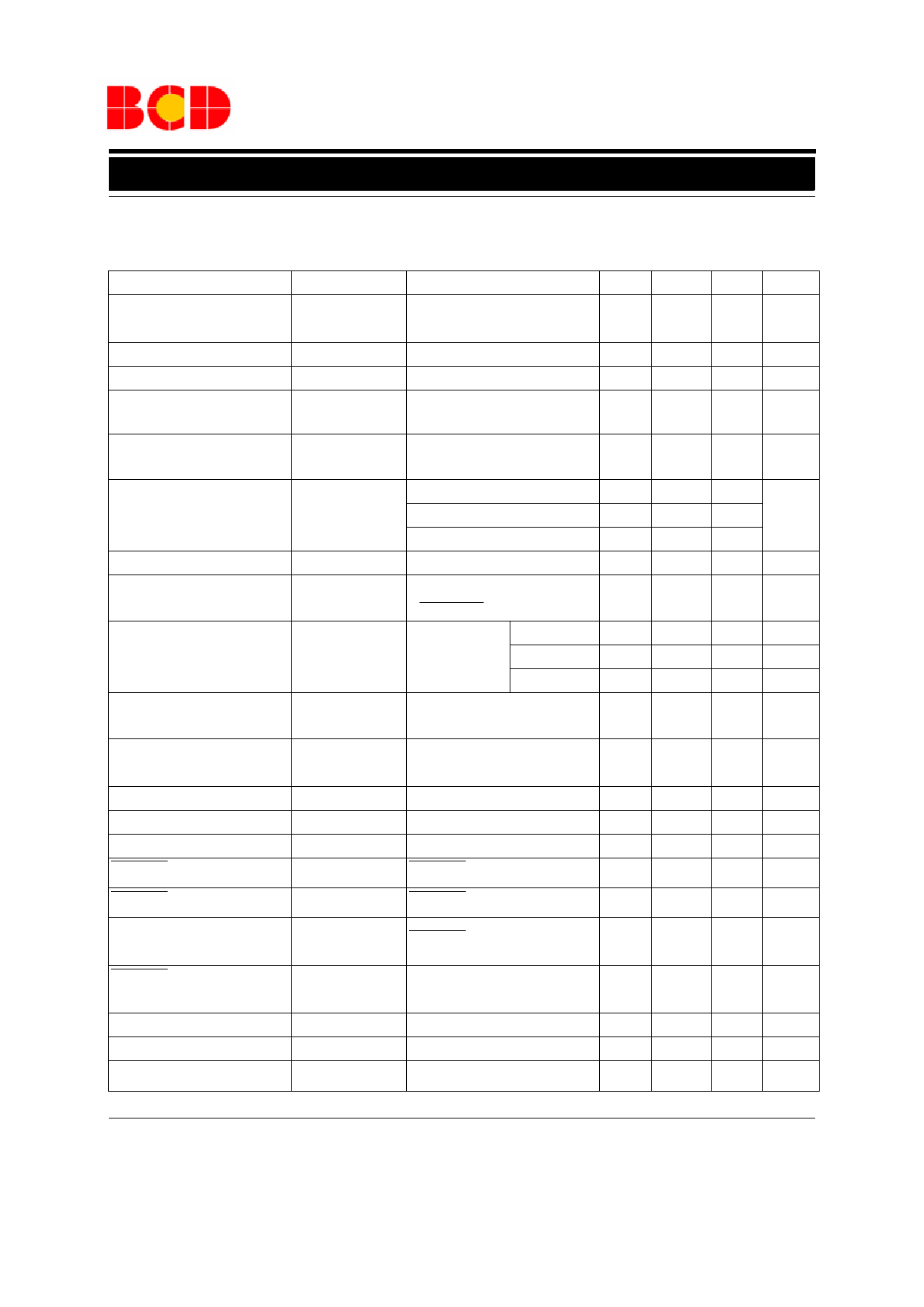
Electrical Characteristics
AP2129-1.0, 1.2 and 3.3 Electrical Characteristics
(CIN=1µF, COUT=1µF, Bold typeface applies over -40oC≤TJ≤85oC, unless otherwise specified.
Parameter
Symbol
Conditions
Min
Output Voltage
VOUT
VIN=VOUT+1V, (Note 2)
1mA≤IOUT≤300mA
98%*
VOUT
Input Voltage
Maximum Output Current
Load Regulation
Line Regulation
VIN
1.8
IOUT(MAX)
∆VOUT
VIN-VOUT=1V, (Note 2)
/(∆IOUT*VOUT) 1mA≤IOUT≤300mA
∆VOUT
VOUT+0.5V≤VIN≤6V, (Note 2)
/(∆VIN*VOUT) IOUT=30mA
Dropout Voltage
Quiescent Current
Standby Current
VDROP
IQ
ISTD
VOUT=1.0V, IOUT=300mA
VOUT=1.2V, IOUT=300mA
VOUT=3.3V, IOUT=300mA
VIN=VOUT+1V, IOUT=0mA
VIN=VOUT+1V,
VSHUTDOWN in off mode
Power Supply
Rejection Ratio
PSRR
Ripple 1Vp-p
VIN=VOUT+1V
f=100Hz
f=1KHz
f=10KHz
Output Voltage
Temperature Coefficient
(∆VOUT/VOUT)
/∆T
IOUT=30mA, -40oC≤TJ≤85oC
Output Current Limit
Short Current Limit
Soft Start Time
RMS Output Noise
Shutdown "High" Voltage
ILIMIT
ISHORT
tUP
VNOISE
VIN-VOUT=1V,
VOUT=0.98*VOUT
VOUT=0V
TA=25oC, 10Hz ≤f≤100kHz
Shutdown input voltage "High" 1.5
Shutdown "Low" Voltage
Shutdown input voltage "Low"
0
VOUT Discharge MOSFET
RDS(ON)
Shutdown input voltage "Low"
Shutdown Pull Down Resis-
tance
Thermal Shutdown
Thermal Shutdown Hysteresis
Typ
450
1400
1200
170
60
0.1
65
65
45
±100
400
50
50
60
60
3
165
30
Max Unit
102%*
VOUT
V
6
V
mA
0.6 %/A
0.06 %/V
1500
1300 mV
300
90
µA
1.0 µA
dB
dB
dB
ppm/oC
mA
mA
µs
µVrms
6
V
0.4
V
Ω
MΩ
oC
oC
Note 2: VIN=1.8V for 1.0 and 1.2 version
Jul. 2008 Rev. 1.0
BCD Semiconductor Manufacturing Limited
6
Share Link: 