APL1117D データシートの表示(PDF) - Anpec Electronics
部品番号
コンポーネント説明
メーカー
APL1117D Datasheet PDF : 11 Pages
| |||

APL1117D/R
Electrical Characteristics
Symbol
Parameter
Test Conditions
VN RMS Output Noise TJ=25°C,10Hz≤F≤10kHz, (% of VOUT)
θth Thermal Resistance Junction to Case, at Tab
Junction to ambient
OT Over Temperature
Point
Quiescent Current TJ=0~125°C,
VIN≤12V
APL1117D/R Unit
Min. Typ. Max.
0.003
%
15
°C/ W
50
150
°C
5.5 10 mA
Note 1: See thermal regulation specifications for changes in output voltage due to heating effects. Load line regulations are mea-
sured at a constant junction temperature by low duty cycle pulse testing.
Note 2: Dropout voltage is specified over the full output current range of the device. Dropout voltage is defined as the minimum input/
output differential measured at the specified output current. Test points and limits are also shown on the Dropout Voltage curve.
Note 3: Minimum load current is defined as the minimum output current required to maintain regulation.
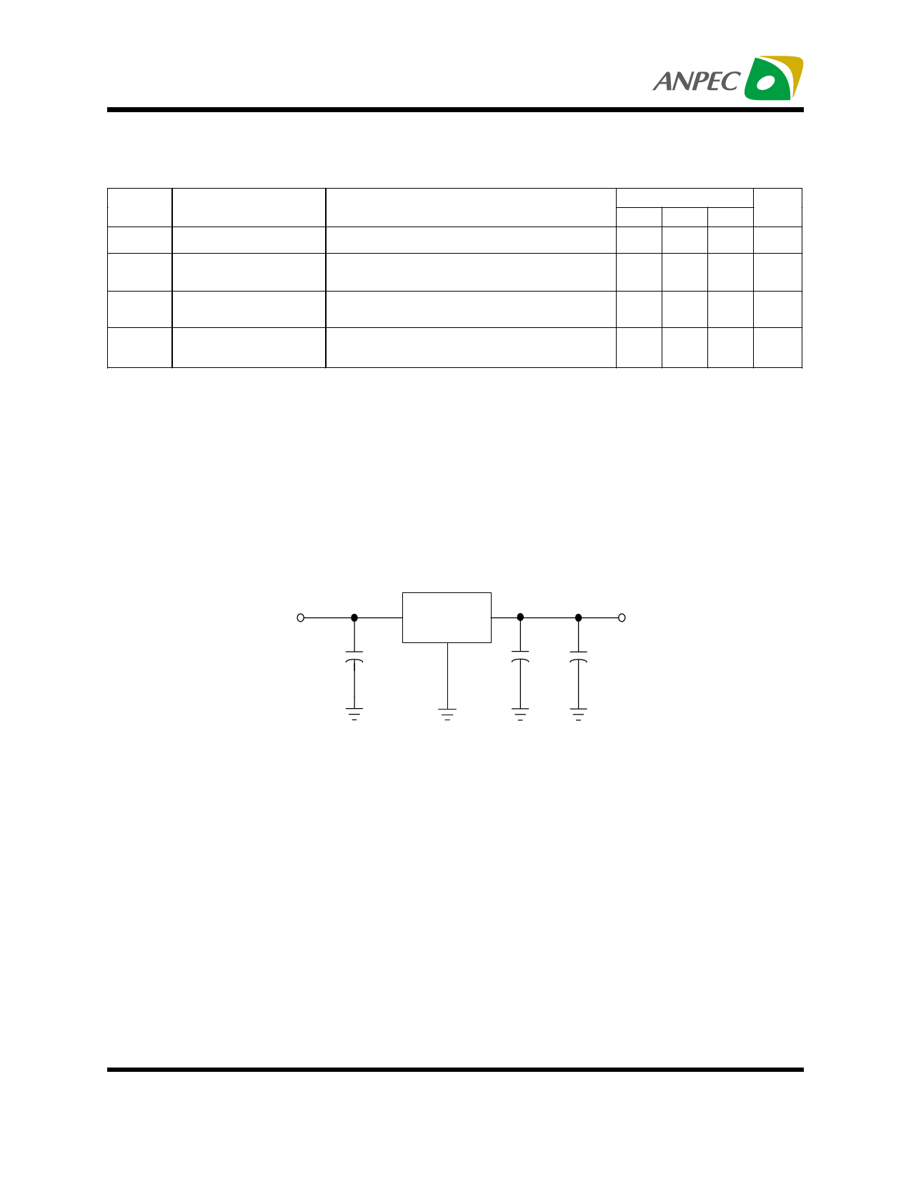
Application Schematic
VIN=5~12V
+ CIN
10uF
APL1117D/R
+ COUT1
0.1uF
VOUT
+ COUT2
10uF
Copyright ANPEC Electronics Corp.
3
Rev. A.3 - Jun., 2003
www.anpec.com.tw