APX9270 データシートの表示(PDF) - Anpec Electronics
部品番号
コンポーネント説明
メーカー
APX9270 Datasheet PDF : 17 Pages
| |||
APX9270
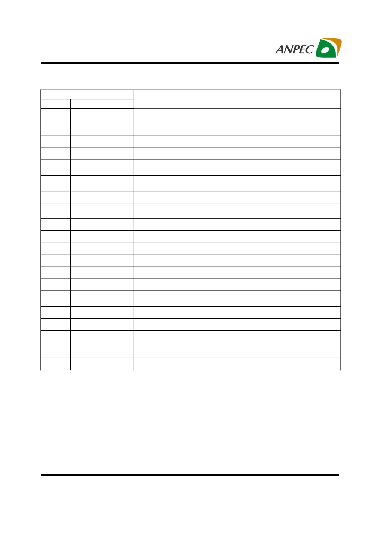
Pin Description
PIN
NO.
NAME
1
PGND
2
OUT2
3
VM
4
VCC
5
OSCH
6
OSCL
7
SET
8
MIN
9
PWM
10
OSC
11
FG
12
IN+
13
HB
14
IN-
15
CT
16
6VREG
17
SGND
18
OUT1
19
PGND
20
PGND
FUNCTION
Power Stage GND.
H-bridge Output Connection. The output stage is a H-bridge formed by four transistors and
four-protection diode for switching applications.
Supply Voltage for Output Stage Input Pin.
Supply Voltage Input Pin.
Setting of the OSC Waveform High Level Voltage. Use a voltage divider from 6VREG to
set OSC waveform high-level voltage.
Setting of the OSC Waveform Low Level Voltage. Use a voltage divider from 6VREG to set
OSC waveform low-level voltage.
Speed Setting. An external voltage into SET pin to set fan speed.
Minimum Speed Setting. Use a voltage divider from 6VREG to set MIN pin voltage for
setting minimum speed.
PWM Signal Input Terminal.
Oscillator Frequency Setting. Connect a capacitor to SGND to set oscillation frequency.
Rotation Speed Output. This is an open-collector output.
Hall Input +. Connect to hell element positive output.
Hall Bias. This is a 1.3V constant-voltage output for hall element bias.
Hall Input -. Connect to hell element negative output.
Shutdown Time and Restart Time Setting. Connect a capacitor to SGND to set shutdown
time and restart time in lock mode.
6V Regulator Output. This is a 6V constant-voltage output for application circuit biases.
Control Stage GND.
H-bridge Output Connection. The output stage is a H-bridge formed by four transistors and
four-protection diode for switching applications.
Power Stage GND.
Power Stage GND.
Copyright © ANPEC Electronics Corp.
7
Rev. A.3 - Jun., 2008
www.anpec.com.tw
Share Link: 