ARM2812TCK データシートの表示(PDF) - International Rectifier
部品番号
コンポーネント説明
メーカー
ARM2812TCK Datasheet PDF : 13 Pages
| |||
ARM28XXT Series
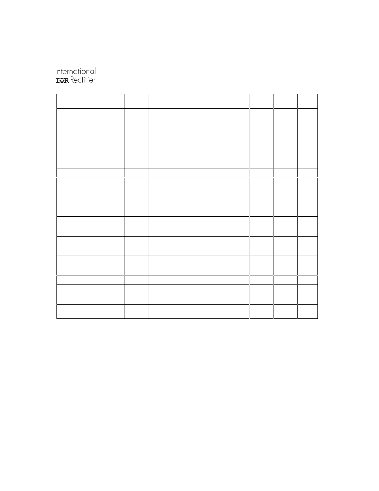
Electrical Performance (Continued)
Parameter
Enable Input
open circuit voltage
drive current (sink)
voltage range
Synchronization Input
frequency range
pulse high level
pulse low level
pulse rise time
pulse duty cycle
Power dissipation, load fault
Output response to step load
changes Notes 7, 11
Recovery time from step load
changes Notes 11, 12
Output response to step line
changes Notes 10, 11
Recovery time from step line
changes Notes 10, 11,13
Turn on overshoot
Turn on delay Note 14
Capacitive load Notes 9, 10
Isolation
Symbol
Conditions
19 Vdc< VIN < 50Vdc
External clock signal on Sync. input (pin 4)
PD Short circuit, any output
10% Load to/from 50% load
VTLD
50% Load to/from 100% load
10% Load to/from 50% load
TTLD
50% Load to/from 100% load
IOUT = 3000 mAdc
VTLN VIN = 19 V to/from 50 V
IOUT = ±500 mAdc
(main)
(dual)
IOUT = 3000 mAdc
TTLN VIN = 19 V to/from 50 V
IOUT = ±500 mAdc
(main)
(dual)
VOS IOUT = minimum and full rated
(main)
(dual)
TDLY IOUT = minimum and full rated
CL No effect on DC performance
(main)
(dual)
ISO 500VDC Input to Output or any pin to case
(except pin 12)
Min
3.0
0.1
-0.5
225
4.5
-0.5
40
20
-200
-200
-350
-1050
5.0
100
Max
Units
5.0
V
mA
50.0
V
310
10.0
0.25
80
7.5
200
200
200
200
350
1050
500
500
500
1500
20
500
100
KHz
V
V
V/µs
%
W
mVPK
µs
mVPK
µs
mV
ms
µF
MΩ
Notes to Specifications Table
1. Operation outside absolute maximum/minimum limits may cause permanent damage to the device. Extended operation at the limits may permanently
degrade performance and affect reliability.
2. Device performance specified in Electrical Performance table is guaranteed when operated within recommended limits. Operation outside
recommended limits is not specified.
3. Parameter measured from 28V to 19 V or to 50V while loads remain fixed.
4. Parameter measured from nominal to minimum or maximum load conditions while line remains fixed.
5. Up to 750 mA is available from the dual outputs provided the total output power does not exceed 30W.
6. Guaranteed for a bandwidth of DC to 20MHz. Tested using a 20KHz to 2MHz bandwidth.
7. Load current is stepped for output under test while other outputs are fixed at half rated load.
8. Load current is fixed for output under test while other output loads are varied for any combination of minimum to maximum.
9. A capacitive load of any value from 0 to the specified maximum is permitted without comprise to DC performance. A capacitive load in excess of the
maximum limit may interfere with the proper operation of the converter’s short circuit protection, causing erratic behavior during turn on.
10. Parameter is tested as part of design characterization or after design or process changes. Thereafter, parameters shall be guaranteed to the limits
specified in the table.
11. Load transient rate of change, di/dt ≤ 2AA/µ/µsS. ec.
12. Recovery time is measured from the initiation of the transient to where VOUT has returned to within ±1% of its steady state value.
13. Line transient rate of change, dv/dt ≤ 50VV/µ/µsS. ec.
14. Turn on delay time is for either a step application of input power or a logical low to high transition on the enable pin (pin 3) while power is present at the
input.
www.irf.com
3
Share Link: 