AS1501 データシートの表示(PDF) - austriamicrosystems AG
部品番号
コンポーネント説明
メーカー
AS1501 Datasheet PDF : 8 Pages
| |||
Data Sheet AS1500/1/2/3
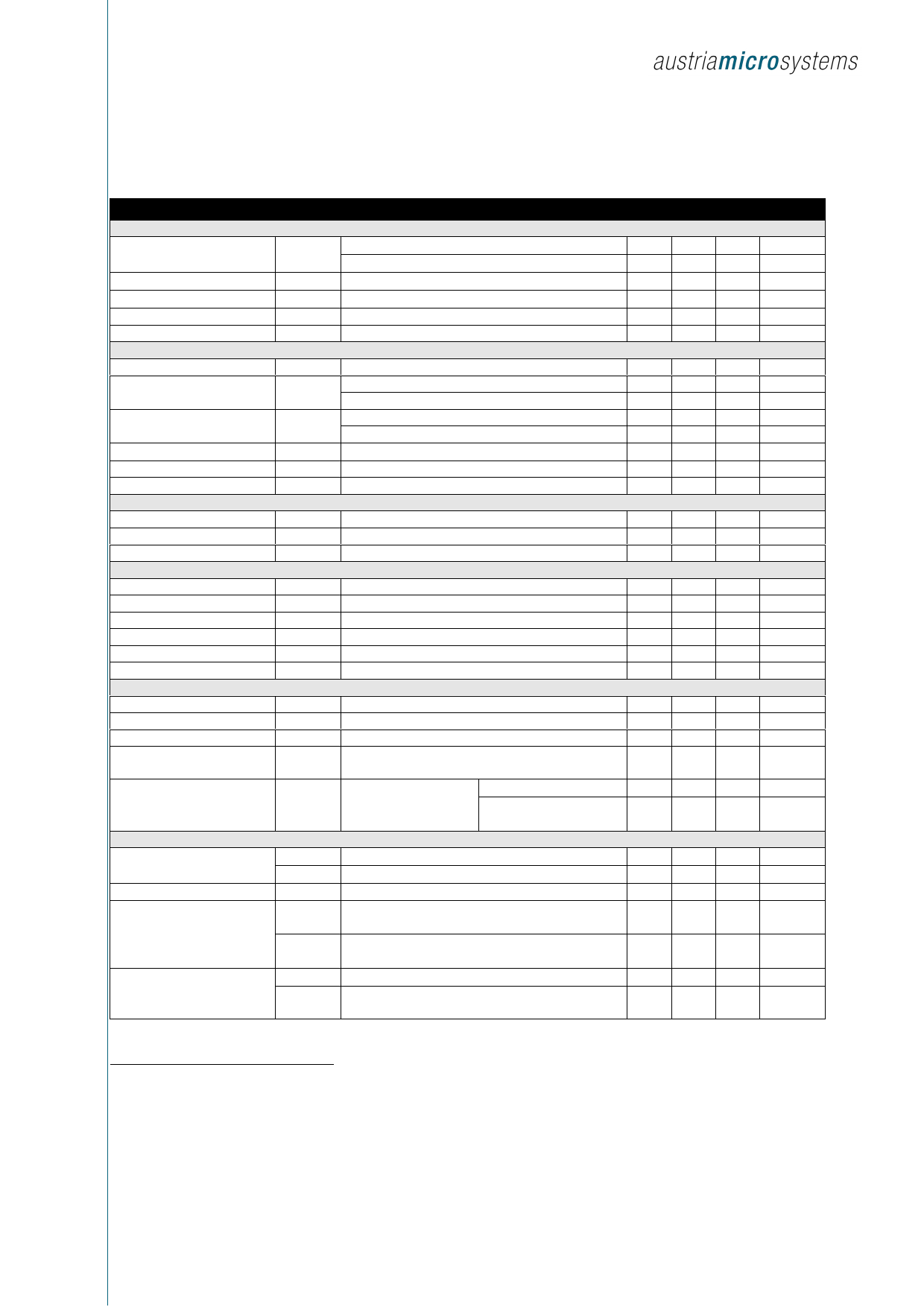
AS1502 / AS1503 – SPECIFICATIONS
VDD = 3V±10% or 5V±10%, VA = VDD, VB = 0V, –40°C ≤ TA ≤ +125°C unless otherwise noted.
ELECTRICAL CHARACTERISTICS – 50k and 100k VERSIONS
Parameter
Symbol
Conditions
Min Typ12 Max Unit
DC CHARACTERISTICS RHEOSTAT MODE
Nominal Resistance13
RAB
TA = 25°C, VDD = 5V, AS1502, Version: 50kΩ 40
TA = 25°C, VDD = 5V, AS1503, Version: 100kΩ 80
50 60
100 120
kΩ
kΩ
Resistance Tempco14
∆RAB/∆T VAB = VDD, Wiper = No Connect
500
ppm/°C
Wiper Resistance
RW VDD = 5V
20 100 200
Ω
Resistor Differential NL15 R-DNL RWB, VDD = 5V, VA = No Connect
Resistor Integral NL
R-INL RWB, VDD = 5V, VA = No Connect
DC CHARACTERISTICS POTENTIOMETER DIVIDER
–1 ±1/4 +1
LSB
–2 ±1/2 +2
LSB
Resolution
N
8
Bits
Integral Nonlinearity
INL
VDD = 5.5V TA = 25°C
VDD = 2.7V TA = 25°C
–4 ±1 +4
LSB
–4 ±1 +4
LSB
Differential Nonlinearity
DNL
VDD = 5.5V TA = 25°C
VDD = 2.7V TA = 25°C
–1 ±1/4 +1
LSB
–1 ±1/4 +1
LSB
Voltage Divider Tempco
Full-Scale Error
Zero-Scale Error
RESISTOR TERMINALS
∆VW /∆T Code = 80H
VWFSE Code = FFH, VDD = 5.5V
VWZSE Code = 00H, VDD = 5.5V
15
–1 –0.25 0
0 0.1 1
ppm/°C
LSB
LSB
Voltage Range16
Capacitance17 Ax, Bx
VA, B, W
CA, B f = 1MHz, Measured to GND, Code = 80H
0
VDD
V
15
pF
Capacitance Wx
CW
DIGITAL INPUTS AND OUTPUTS
f = 1MHz, Measured to GND, Code = 80H
80
pF
Input Logic High
Input Logic Low
Input Logic High
Input Logic Low
Input Current
Input Capacitance
POWER SUPPLIES
VIH
VIL
VIH
VIL
IIH, IIL
CIL
VDD = 5V
VDD = 5V
VDD = 3V
VDD = 3V
VIN = 5V or 0V, VDD = 5V
2.4
V
0.8
V
2.1
V
0.6
V
±1
µA
5
pF
Power Supply Range
VDD
2.7
5.5
V
Supply Current (CMOS)
IDD VIH = VDD or VIL = 0V, VDD = 5.5V
0.1 1
µA
Supply Current (TTL)18
IDD VIH = 2.4V or 0.8V, VDD = 5.5V
0.9 4
mA
Power Dissipation
(CMOS)19
PDISS VIH = VDD or VIL = 0V, VDD = 5.5V
27.5 µW
Power Supply Suppression
Ratio
PSSR
VDD = 5V + 0.5VP
sine wave @ 1kHz
AS1502, Version: 50kΩ
AS1503, Version:
100kΩ
-43 tbd.
dB
-48 tbd.
dB
DYNAMIC CHARACTERISTICS20
Bandwidth –3dB
Bandwidth –3dB
Total Harmonic Distortion
BW_50k RWB = 50kΩ, VDD = 5V
BW_100k RWB = 100kΩ, VDD = 5V
THDW VA = 1VRMS + 2VDC, VB = 2VDC, f = 1kHz
220
kHz
110
kHz
0.003
%
VW Settling Time
tS_50k
tS_100k
RWB = 50kΩ, VA = VDD, VB = 0V, ±1% Error
Band
RWB = 100kΩ, VA = VDD, VB = 0V, ±1% Error
Band
9
18
µs
µs
Resistor Noise Voltage
eNWB_50k RWB = 50kΩ, f = 1kHz
eNWB_100
k
RWB = 100kΩ, f = 1kHz
20
nV/ √ Hz
29
nV/ √ Hz
Table 4: Electrical Characteristics – 50k and 100k Versions
12 Typicals represent average readings at 25°C and VDD = 5V.
13 Wiper is not connected. IAB = 70µA for the 50kΩ version and 35µA for the 100kΩ version.
14 All Tempcos are guaranteed by design and not subject to production test.
15 Terminal A is not connected. IW = 70µA for the 50kΩ version and 35µA for the 100kΩ version.
16 Resistor terminals A, B, W have no limitations on polarity with respect to each other.
17 All capacitances are guaranteed by design and not subject to production test. Resistor-terminal capacitance tests are measured with 2.5V
bias on the measured terminal. The remaining resistor terminals are left open circuit.
18 Worst-case supply current consumed when input logic level at 2.4V, standard characteristic of CMOS logic.
19 PDISS is calculated from (IDD×VDD). CMOS logic level inputs result in minimum power dissipation.
20 All dynamic characteristics are guaranteed by design and not subject to production test. All dynamic characteristics use VDD=5V.
Revision 1.0, Oct 2004
Page 4 of 8
Share Link: 