AS1341 データシートの表示(PDF) - austriamicrosystems AG
部品番号
コンポーネント説明
メーカー
AS1341 Datasheet PDF : 18 Pages
| |||
AS1341
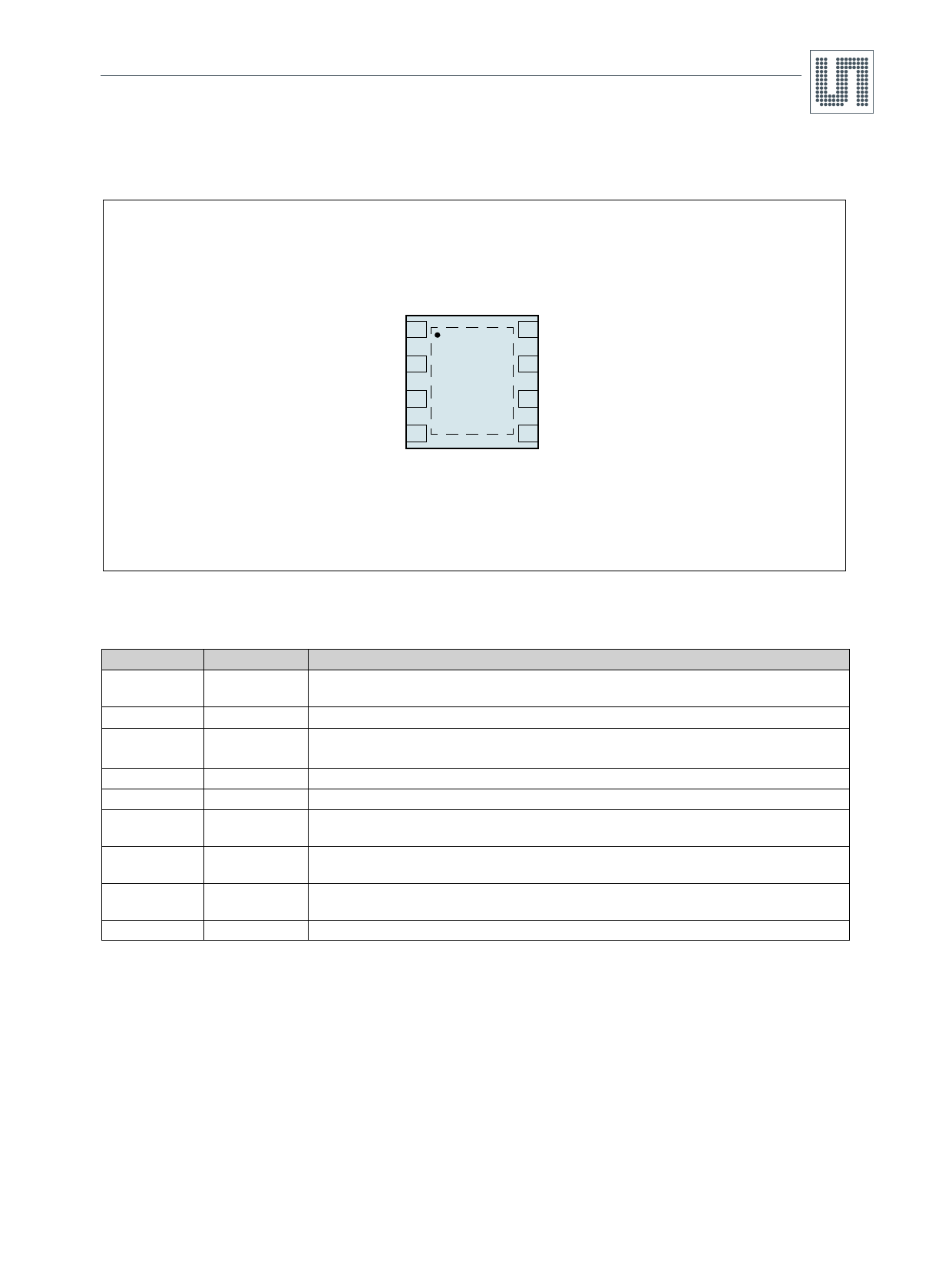
Datasheet - Pin Assignments
4 Pin Assignments
Figure 2. Pin Assignments (Top View)
FB 1
GND 2
POK 3
LX 4
8 OUT
AS1341
7 SHDNN
6 ILIMIT
9 5 IN
4.1 Pin Descriptions
Table 1. Pin Descriptions
Pin Number
Pin Name
1
FB
2
GND
3
POK
4
LX
5
IN
6
ILIMIT
7
SHDNN
8
OUT
9
NC
Description
Feedback Input. For the fixed 5V output connect this pin to GND. For adjustable output, connect to a
resistive divider between VOUT and GND to set the output voltage between 1.25V and VIN.
Ground
Power OK. Active-low open-drain reset output.
Note: Connect pin POK to GND when the Power-Ok feature is not used.
Inductor Connection. Connect this pin to an external inductor.
4.5V to 20V Input Supply Voltage
Peak Current Control Input. Connect this pin to IN or GND to set peak current limit (see Setting
Current Limit on page 11).
Shutdown Input. A low on this pin puts the AS1341 into shutdown mode. Supply current is reduced to
0.8µA and LX goes high-impedance.
Regulated Output Voltage High-Impedance Sense Input. For the fixed 5V output connect this pin to
VOUT. For adjustable output connect this pin to GND.
Exposed Pad. This pad is not connected internally. Connect to GND or do not connect.
www.ams.com/DC-DC_Step-Up/AS1341
Revision 1.09
2 - 18
Share Link: 