AT24C04B データシートの表示(PDF) - Atmel Corporation
部品番号
コンポーネント説明
メーカー
AT24C04B
Atmel Corporation

AT24C04B Datasheet PDF : 20 Pages
| |||
6. Device Operation
CLOCK and DATA TRANSITIONS: The SDA pin is normally pulled high with an external device.
Data on the SDA pin may change only during SCL low time periods (see Figure 8-2 on page 8).
Data changes during SCL high periods will indicate a start or stop condition as defined below.
START CONDITION: A high-to-low transition of SDA with SCL high is a start condition which
must precede any other command (see Figure 8-3 on page 8).
STOP CONDITION: A low-to-high transition of SDA with SCL high is a stop condition. After a
read sequence, the stop command will place the EEPROM in a standby power mode (see Fig-
ure 8-3 on page 8).
ACKNOWLEDGE: All addresses and data words are serially transmitted to and from the
EEPROM in 8-bit words. The EEPROM sends a “0” to acknowledge that it has received each
word. This happens during the ninth clock cycle.
STANDBY MODE: The AT24C01B/02B/04B/08B features a low-power standby mode which is
enabled: (a) upon power-up and (b) after the receipt of the STOP bit and the completion of any
internal operations.
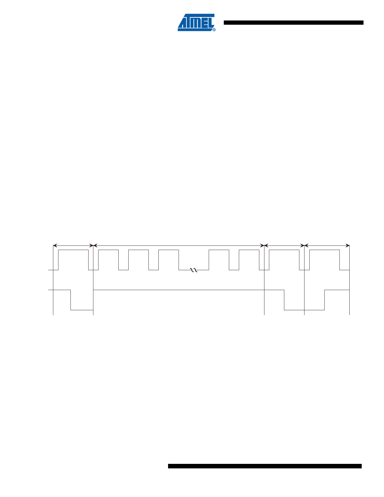
2-WIRE SOFTWARE RESET: After an interruption in protocol, power loss or system reset, any
2-wire part can be protocol reset by following these steps: (a) Create a start bit condition, (b)
clock 9 cycles, (c) create another start but followed by stop bit condition as shown below. The
device is ready for next communication after above steps have been completed.
Figure 6-1. Software Reset
Start bit
Dummy Clock Cycles
Start bit
Stop bit
SCL
1
2
3
8
9
SDA
6 AT24C01B/02B/04B/08B
8517C–SEEPR–01/09
Share Link: