AT24C01BN-SH-T(2008) データシートの表示(PDF) - Atmel Corporation
部品番号
コンポーネント説明
メーカー
AT24C01BN-SH-T Datasheet PDF : 25 Pages
| |||
AT24C01B
1. Pin Description
SERIAL CLOCK (SCL): The SCL input is used to positive edge clock data into each EEPROM
device and negative edge clock data out of each device.
SERIAL DATA (SDA): The SDA pin is bidirectional for serial data transfer. This pin is open-
drain driven and may be wire-ORed with any number of other open-drain or open-collector
devices.
DEVICE/PAGE ADDRESSES (A2, A1, A0): The A2, A1 and A0 pins are device address inputs
that are hard wired for the AT24C01B. As many as eight 1K devices may be addressed on a sin-
gle bus system (device addressing is discussed in detail under the Device Addressing section).
WRITE PROTECT (WP): The AT24C01B has a write protect pin that provides hardware data
protection. The write protect pin allows normal read/write operations when connected to ground
(GND). When the write protect pin is connected to VCC, the write protection feature is enabled
and operates as shown in Table 1-1.
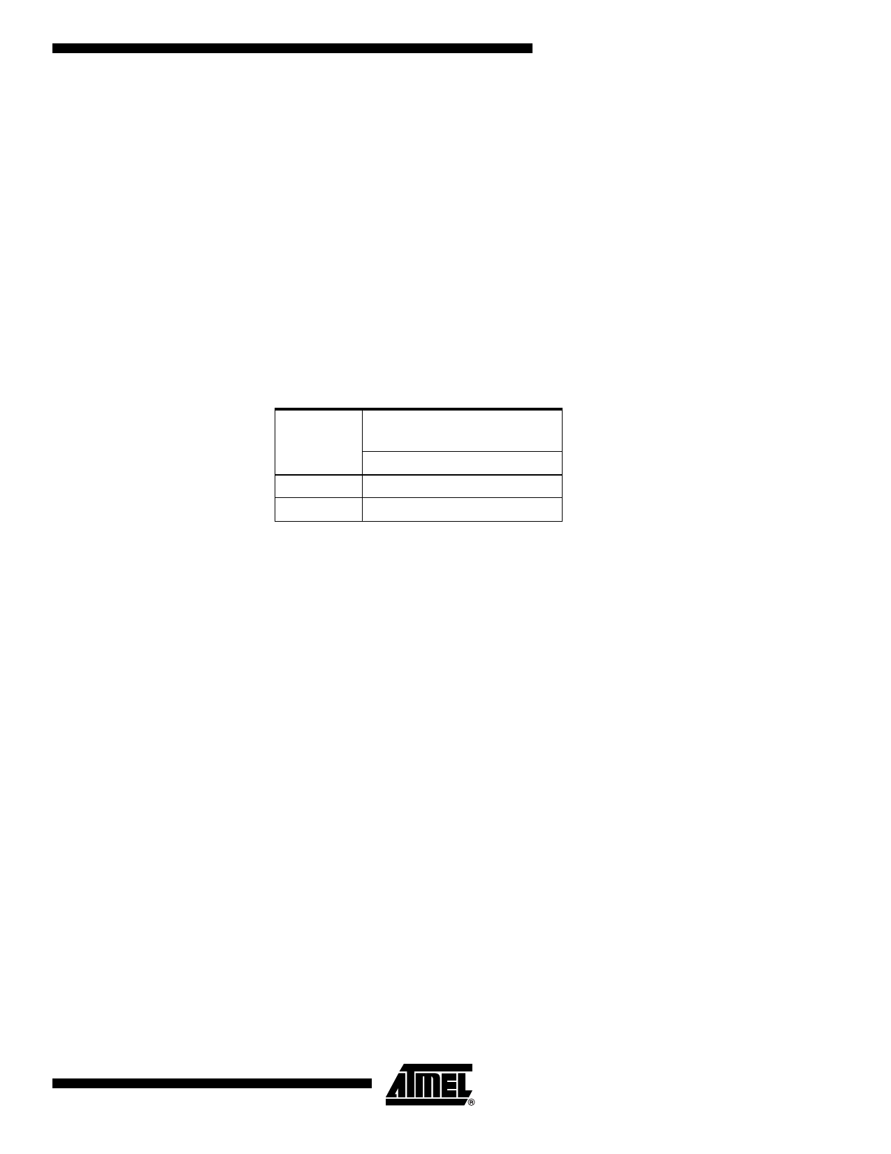
Table 1-1.
WP Pin
Status
At VCC
At GND
Write Protect
Part of the Array Protected
24C01B
Full (1K) Array
Normal Read/Write Operations
2. Memory Organization
AT24C01B, 1K SERIAL EEPROM: Internally organized with 16 pages of 8 bytes each, the 1K
requires an 7-bit data word address for random word addressing. (See Figure 8-2 on page 10)
3
5156E–SEEPR–10/08
Share Link: 