AT24C08B-TH-B データシートの表示(PDF) - Atmel Corporation
部品番号
コンポーネント説明
メーカー
AT24C08B-TH-B Datasheet PDF : 26 Pages
| |||
AT24C04B/08B
1. Pin Description
SERIAL CLOCK (SCL): The SCL input is used to positive edge clock data into each EEPROM
device and negative edge clock data out of each device.
SERIAL DATA (SDA): The SDA pin is bidirectional for serial data transfer. This pin is open-
drain driven and may be wire-ORed with any number of other open-drain or open-collector
devices.
DEVICE/PAGE ADDRESSES (A2, A1, A0):
The AT24C04B uses the A2 and A1 inputs for hard wire addressing and a toal of four 4K devices
may be addressed on a single bus system. The A0 pin is a no connect and can be connected to
ground (device addressing is discussed in detail under the Device Addressing section).
The AT24C08B only uses the A2 input for hardware addressing and a total of two 8K devices
may be addressed on a single bus system. The A0 and A1 pins are no connects and can be
connected to ground (device addressing is discussed in detail under the Device Addressing
section).
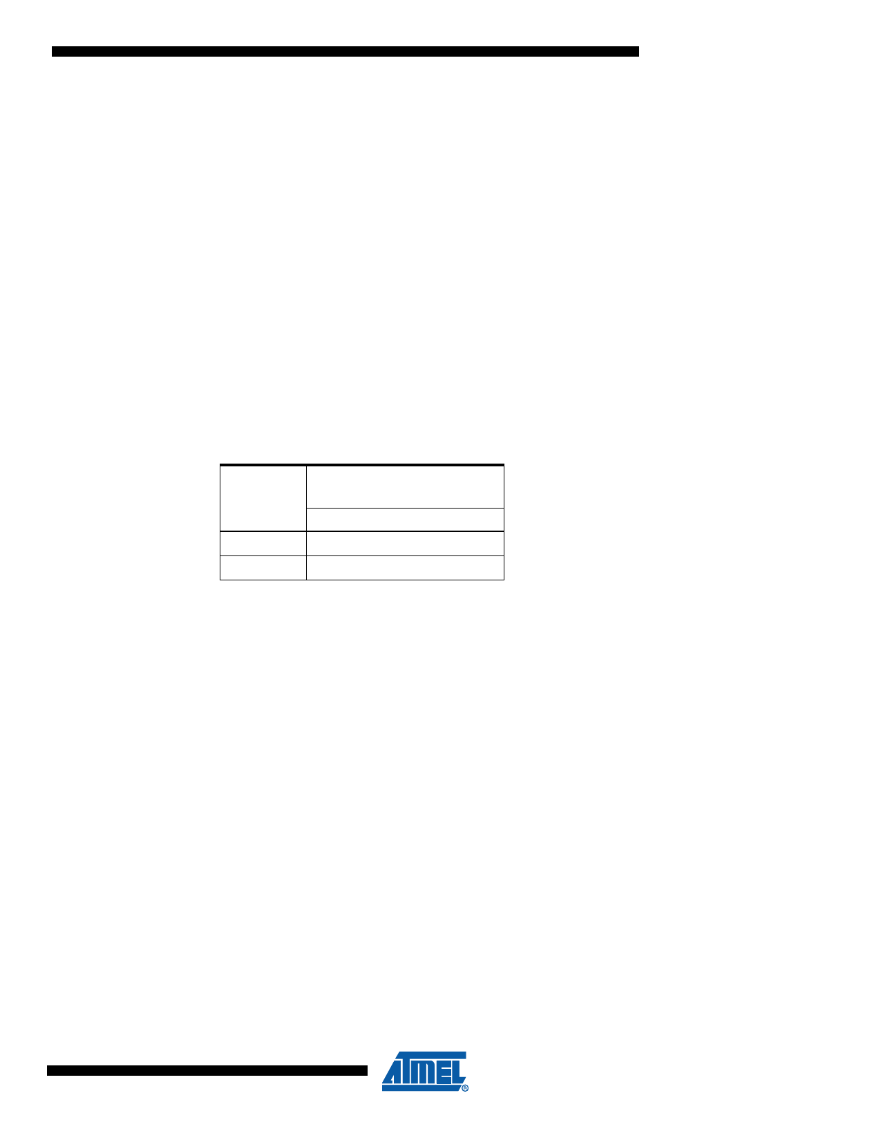
Table 1-1.
WP Pin
Status
At VCC
At GND
Write Protect
Part of the Array Protected
24C04B/08B
Full Array
Normal Read/Write Operations
3
5226D–SEEPR–7/08
Share Link: 