AT24C01A-10TSI-2.7 データシートの表示(PDF) - Atmel Corporation
部品番号
コンポーネント説明
メーカー
AT24C01A-10TSI-2.7
Atmel Corporation

AT24C01A-10TSI-2.7 Datasheet PDF : 21 Pages
| |||
Absolute Maximum Ratings
Operating Temperature .................................. -55°C to +125°C
Storage Temperature ..................................... -65°C to +150°C
Voltage on Any Pin
with Respect to Ground .....................................-1.0V to +7.0V
Maximum Operating Voltage........................................... 6.25V
DC Output Current........................................................ 5.0 mA
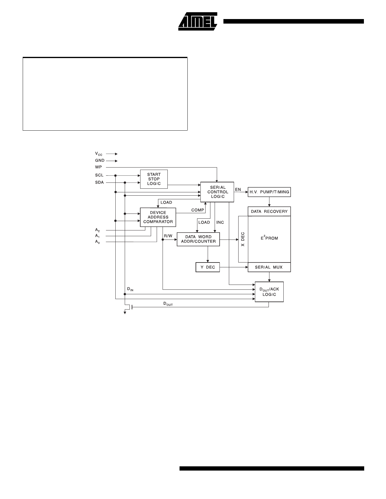
Block Diagram
*NOTICE:
Stresses beyond those listed under “Absolute
Maximum Ratings” may cause permanent dam-
age to the device. This is a stress rating only and
functional operation of the device at these or any
other conditions beyond those indicated in the
operational sections of this specification is not
implied. Exposure to absolute maximum rating
conditions for extended periods may affect device
reliability.
Pin Description
SERIAL CLOCK (SCL): The SCL input is used to positive
edge clock data into each EEPROM device and negative
edge clock data out of each device.
SERIAL DATA (SDA): The SDA pin is bidirectional for
serial data transfer. This pin is open-drain driven and may
be wire-ORed with any number of other open-drain or open
collector devices.
DEVICE/PAGE ADDRESSES (A2, A1, A0): The A2, A1
and A0 pins are device address inputs that are hard wired
for the AT24C01A and the AT24C02. As many as eight
1K/2K devices may be addressed on a single bus system
(device addressing is discussed in detail under the Device
Addressing section).
The AT24C04 uses the A2 and A1 inputs for hard wire
addressing and a total of four 4K devices may be
addressed on a single bus system. The A0 pin is a no con-
nect.
The AT24C08 only uses the A2 input for hardwire address-
ing and a total of two 8K devices may be addressed on a
single bus system. The A0 and A1 pins are no connects.
The AT24C16 does not use the device address pins which
limits the number of devices on a single bus to one. The
A0, A1 and A2 pins are no connects.
WRITE PROTECT (WP): The AT24C01A/02/04/16 has a
Write Protect pin that provides hardware data protection.
The Write Protect pin allows normal read/write operations
when connected to ground (GND). When the Write Protect
pin is connected to VCC, the write protection feature is
enabled and operates as shown in the following table.
2
AT24C01A/02/04/08/16
Share Link: