AT24C01A-10TSI-2.7 データシートの表示(PDF) - Atmel Corporation
部品番号
コンポーネント説明
メーカー
AT24C01A-10TSI-2.7
Atmel Corporation

AT24C01A-10TSI-2.7 Datasheet PDF : 21 Pages
| |||
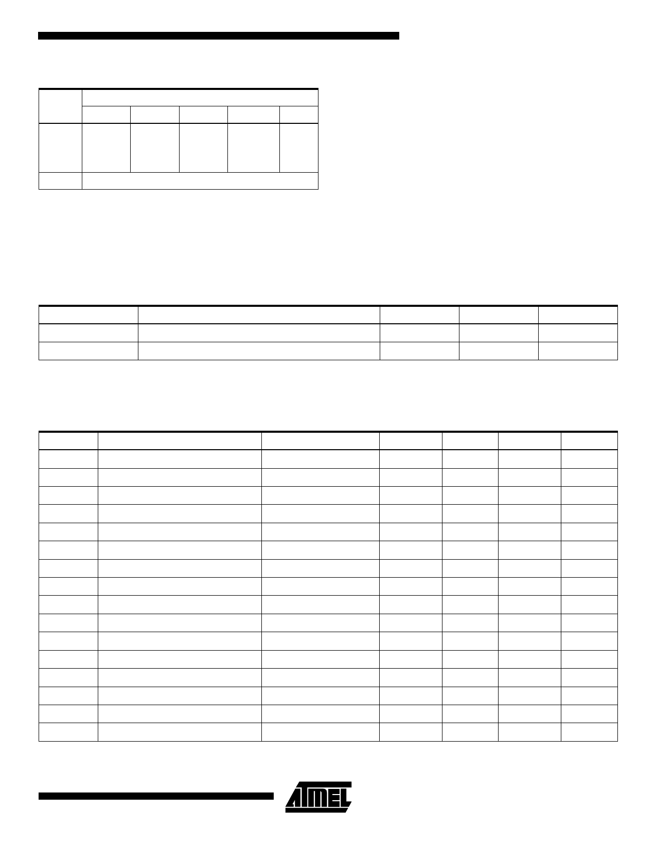
AT24C01A/02/04/08/16
WP Pin
Status
At VCC
At GND
Part of the Array Protected
24C01A 24C02
24C04
24C08
Full (1K)
Array
Full (2K)
Array
Full (4K)
Array
Normal
Read/
Write
Operation
Normal Read/Write Operations
24C16
Upper
Half
(8K)
Array
Memory Organization
AT24C01A, 1K SERIAL EEPROM: Internally organized
with 128 pages of 1-byte each, the 1K requires a 7-bit data
word address for random word addressing.
AT24C02, 2K SERIAL EEPROM: Internally organized with
256 pages of 1-byte each, the 2K requires an 8-bit data
word address for random word addressing.
AT24C04, 4K SERIAL EEPROM: The 4K is internally
organized with 256 pages of 2 bytes each. Random word
addressing AT24C01A/02/04/08/16 requires a 9-bit data
word address.
AT24C08, 8K SERIAL EEPROM: The 8K is internally
organized with 4 blocks of 256 pages of 4 bytes each. Ran-
dom word addressing requires a 10-bit data word address.
AT24C16, 16K SERIAL EEPROM: The 16K is internally
organized with 8 blocks of 256 pages of 8 bytes each. Ran-
dom word addressing requires an 11-bit data word
address.
Pin Capacitance(1)
Applicable over recommended operating range from TA = 25°C, f = 1.0 MHz, VCC = +1.8V.
Symbol
Test Condition
Max
Units
Conditions
CI/O
CIN
Note:
Input/Output Capacitance (SDA)
Input Capacitance (A0, A1, A2, SCL)
1. This parameter is characterized and is not 100% tested.
8
pF
VI/O = 0V
6
pF
VIN = 0V
DC Characteristics
Applicable over recommended operating range from: TAI = -40°C to +85°C, VCC = +1.8V to +5.5V, TAC = 0°C to +70°C,
VCC = +1.8V to +5.5V (unless otherwise noted).
Symbol Parameter
Test Condition
Min
Typ
Max
Units
VCC1
Supply Voltage
1.8
5.5
V
VCC2
Supply Voltage
2.5
5.5
V
VCC3
Supply Voltage
2.7
5.5
V
VCC4
Supply Voltage
4.5
5.5
V
ICC
Supply Current VCC = 5.0V
READ at 100 kHz
0.4
1.0
mA
ICC
Supply Current VCC = 5.0V
WRITE at 100 kHz
2.0
3.0
mA
ISB1
Standby Current VCC = 1.8V
VIN = VCC or VSS
0.6
3.0
µA
ISB2
Standby Current VCC = 2.5V
VIN = VCC or VSS
1.4
4.0
µA
ISB3
Standby Current VCC = 2.7V
VIN = VCC or VSS
1.6
4.0
µA
ISB4
Standby Current VCC = 5.0V
VIN = VCC or VSS
8.0
18.0
µA
ILI
Input Leakage Current
VIN = VCC or VSS
0.10
3.0
µA
ILO
Output Leakage Current
VOUT = VCC or VSS
0.05
3.0
µA
VIL
Input Low Level(1)
-0.6
VCC x 0.3
V
VIH
Input High Level(1)
VCC x 0.7
VCC + 0.5
V
VOL2
Output Low Level VCC = 3.0V
IOL = 2.1 mA
0.4
V
VOL1
Output Low Level VCC = 1.8V
IOL = 0.15 mA
Note: 1. VIL min and VIH max are reference only and are not tested.
0.2
V
3
Share Link: