AT24C01A-10TSI-2.7 データシートの表示(PDF) - Atmel Corporation
部品番号
コンポーネント説明
メーカー
AT24C01A-10TSI-2.7
Atmel Corporation

AT24C01A-10TSI-2.7 Datasheet PDF : 21 Pages
| |||
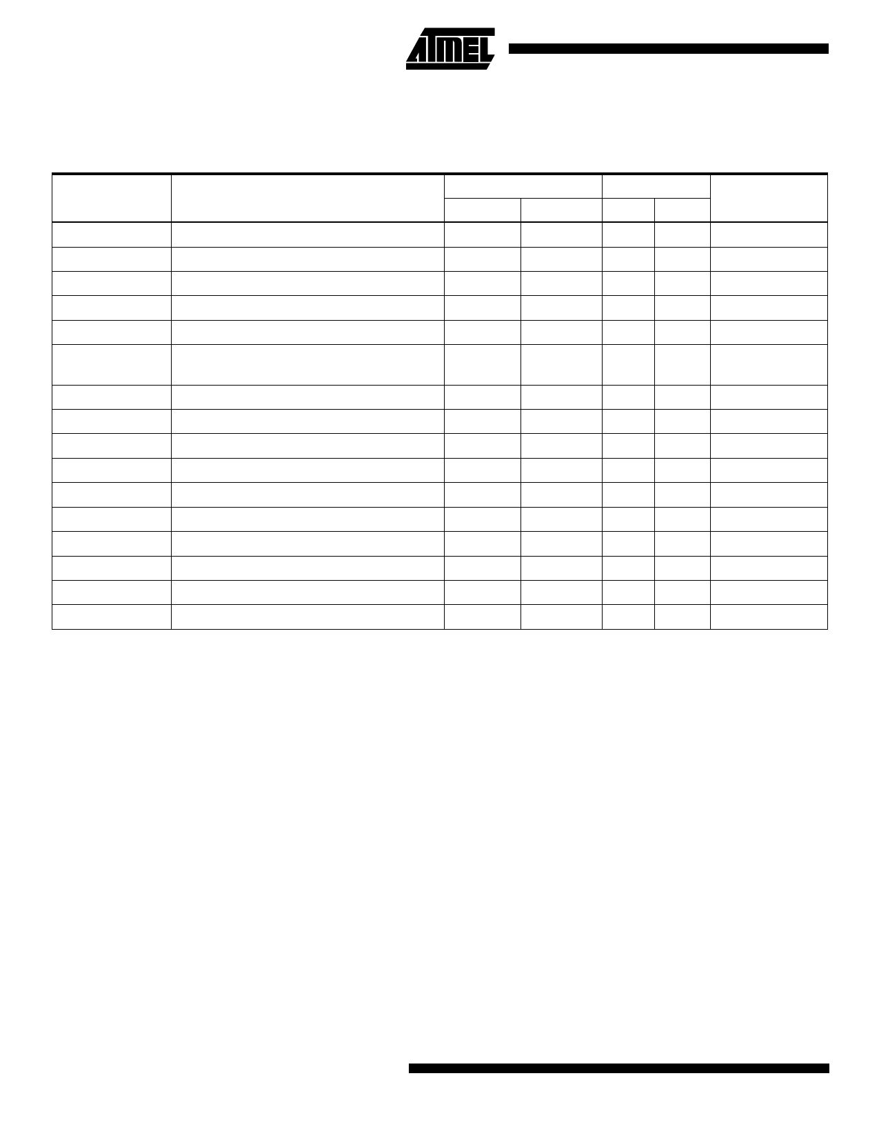
AC Characteristics
Applicable over recommended operating range from TA = -40°C to +85°C, VCC = +1.8V to +5.5V, CL = 1 TTL Gate and
100pF (unless otherwise noted).
2.7-, 2.5-, 1.8-volt
5.0-volt
Symbol
Parameter
Min
Max
Min Max
Units
fSCL
tLOW
tHIGH
tI
tAA
tBUF
Clock Frequency, SCL
Clock Pulse Width Low
Clock Pulse Width High
Noise Suppression Time(1)
Clock Low to Data Out Valid
Time the bus must be free before
a new transmission can start(1)
100
400
kHz
4.7
1.2
µs
4.0
0.6
µs
100
50
ns
0.1
4.5
0.1
0.9
µs
4.7
1.2
µs
tHD.STA
Start Hold Time
4.0
tSU.STA
Start Set-up Time
4.7
tHD.DAT
Data In Hold Time
0
tSU.DAT
Data In Set-up Time
200
tR
Inputs Rise Time(1)
tF
Inputs Fall Time(1)
tSU.STO
Stop Set-up Time
4.7
tDH
Data Out Hold Time
100
tWR
Write Cycle Time
Endurance(1)
5.0V, 25°C, Page Mode
1M
Note: 1. This parameter is characterized and is not 100% tested.
0.6
µs
0.6
µs
0
µs
100
ns
1.0
0.3
µs
300
300
ns
0.6
µs
50
ns
10
10
ms
1M
Write Cycles
Device Operation
CLOCK and DATA TRANSITIONS: The SDA pin is nor-
mally pulled high with an external device. Data on the SDA
pin may change only during SCL low time periods (refer to
Data Validity timing diagram). Data changes during SCL
high periods will indicate a start or stop condition as
defined below.
START CONDITION: A high-to-low transition of SDA with
SCL high is a start condition which must precede any other
command (refer to Start and Stop Definition timing dia-
gram).
STOP CONDITION: A low-to-high transition of SDA with
SCL high is a stop condition. After a read sequence, the
stop command will place the EEPROM in a standby power
mode (refer to Start and Stop Definition timing diagram).
ACKNOWLEDGE: All addresses and data words are seri-
ally transmitted to and from the EEPROM in 8-bit words.
The EEPROM sends a zero to acknowledge that it has
received each word. This happens during the ninth clock
cycle.
STANDBY MODE: The AT24C01A/02/04/08/16 features a
low power standby mode which is enabled: (a) upon power-
up and (b) after the receipt of the STOP bit and the comple-
tion of any internal operations.
MEMORY RESET: After an interruption in protocol, power
loss or system reset, any 2-wire part can be reset by follow-
ing these steps:
1. Clock up to 9 cycles.
2. Look for SDA high in each cycle while SCL is high.
3. Create a start condition as SDA is high.
4
AT24C01A/02/04/08/16
Share Link: