24C21 データシートの表示(PDF) - Atmel Corporation
部品番号
コンポーネント説明
メーカー
24C21 Datasheet PDF : 13 Pages
| |||
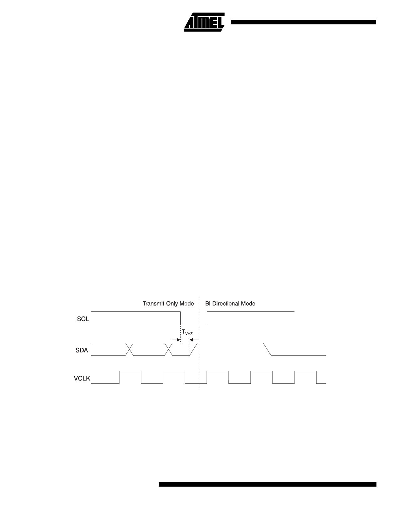
Bidirectional Mode (DDC2)
This mode supports a 2-wire, Bidirectional data transmis-
sion protocol. The AT24C21 can be switched into the Bidi-
rectional Mode by issuing a valid high to low transition on
the SCL pin (refer to Figure 3). After the device is in the
Bidirectional Mode, all inputs to the VCLK pin are ignored,
except when a logic high is required to enable write capa-
bility. All byte and page writes and byte and sequential
reads are supported in this mode.
Bidirectional Mode Operation
CLOCK and DATA TRANSITIONS: The SDA pin is nor-
mally pulled high with an external device. Data on the SDA
pin may change only during SCL low time periods (refer to
Data Validity timing diagram). Data changes during SCL
high periods will indicate a start or stop condition as
defined below.
START CONDITION: A high-to-low transition of SDA with
SCL high is a start condition which must precede any other
command (refer to Start and Stop Definition timing dia-
gram).
STOP CONDITION: A low-to-high transition of SDA with
SCL high is a stop condition. After a read or write
sequence, the stop command will place the EEPROM in a
standby power mode (refer to Start and Stop Definition tim-
ing diagram).
ACKNOWLEDGE: All addresses and data words are seri-
ally transmitted to and from the EEPROM in 8-bit words.
The EEPROM sends a zero to acknowledge that it has
received each word. This happens during the ninth clock
cycle.
Device Addressing
The AT24C21 requires an 8-bit device address word fol-
lowing a start condition to enable the chip for a read or
write operation (refer to Figure 4).
The device address word consists of a mandatory one,
zero sequence for the first four most significant bits as
shown. This is common to all the EEPROM devices.
The next three bits are don’t care for the AT24C21.
The eighth bit of the device address is the read/write opera-
tion select bit. A read operation is initiated if this bit is high
and a write operation is initiated if this bit is low.
Upon a compare of the device address, the EEPROM will
output a zero. If a compare is not made, the chip will return
to a standby state.
STANDBY MODE: The AT24C21 features a low power
standby mode which is enabled: (a) upon power-up and (b)
after the receipt of the STOP bit and the completion of any
internal operations.
MEMORY RESET: After an interruption in protocol, power
loss or system reset, any 2-wire part can be reset by follow-
ing these steps:
(a) Clock up to 9 cycles, (b) look for SDA high in each cycle
while SCL is high and then (c) create a start condition as
SDA is high.
Figure 3. Mode Transition
6
AT24C21
Share Link: 