NX25M041A-3V-R データシートの表示(PDF) - NexFlash -> Winbond Electronics
部品番号
コンポーネント説明
メーカー
NX25M041A-3V-R
NexFlash -> Winbond Electronics

NX25M041A-3V-R Datasheet PDF : 7 Pages
| |||
NX25Mxxx
NX26Mxxx
Vcc
C1
(4) (1)
A3-1*
C2 (11)
A3
A0
#1
1
Vcc
#0
SERIAL I/O,
AND GENERAL
A3-0
C4 (11)
A3
PURPOSE
PORT PINS
SCK
SIO
A1
C3 (2)
C7 (3)
C8 (13)
SCK
SIO
A1
Serial Flash
Memory
NXS Interface
2
A2, WP/DT
C6 (12)
A2
26Fxxx Series
Vcc C1
C5 GND
Detect Control* 10K
WPS
A3-1
C2 DT C6 A2 & WP/DT
MICROCONTROLLER
C5
GND
A0
SCK C3
A3-0 C4
C7 SIO
C8 A1
BOTTOM VIEW
(CONTACT SIDE)
3
(14)
(1)
(DSP or ASIC)
* OPTIONAL
A3-0
SCK
A3-1
Vcc
A1
A3-0
C4
C8 A1
TOP VIEW
SIO
SCK C3
C7 SIO
(LABEL SIDE)
4
A2 & WP/DT A3-1
C2 DT C6 A2 & WP/DT
GND
Vcc
C1
C5 GND
NXD012A-0598
5
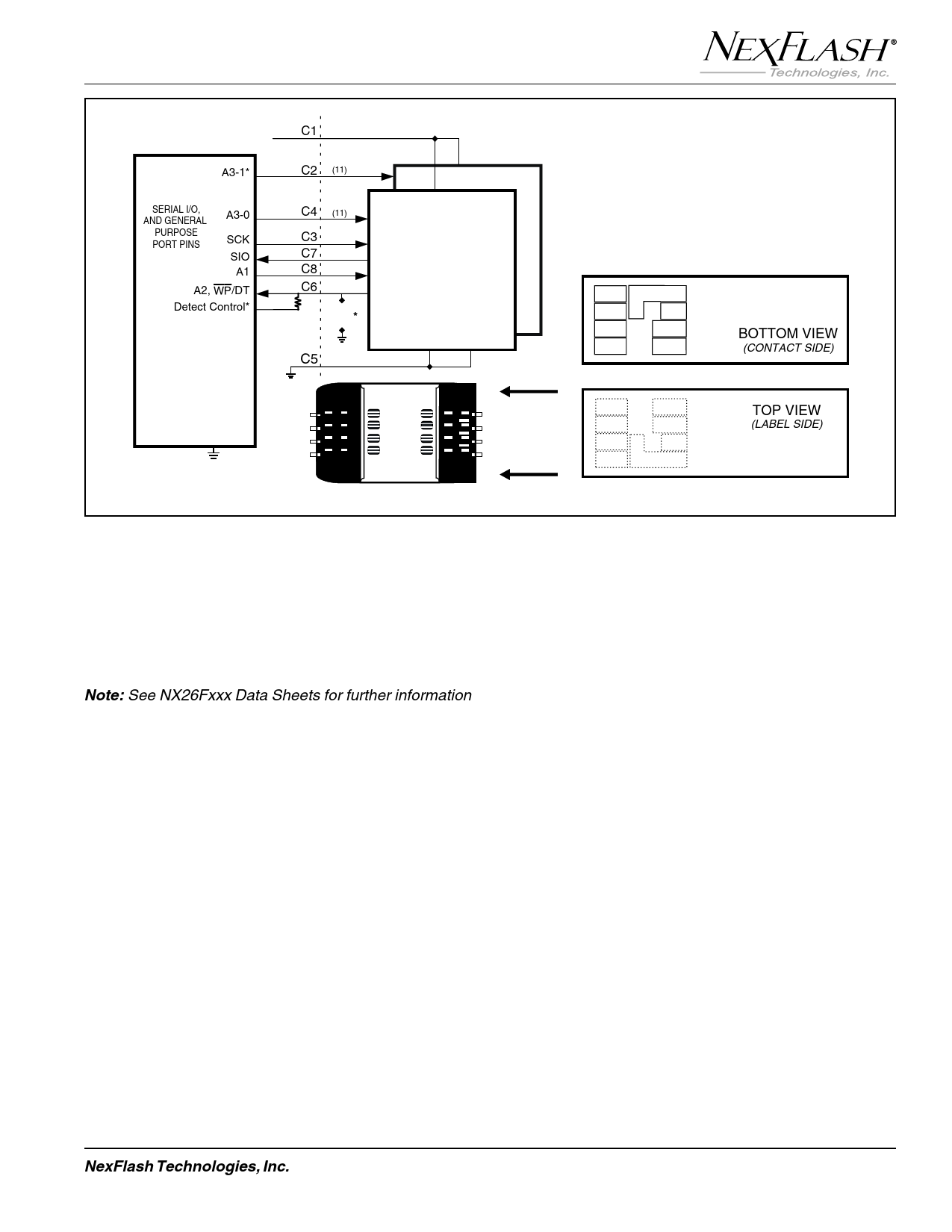
Figure 3. Typical interface for Serial Flash Module with NXS Interface using NX26Fxxx Series Devices.
6 Equivalent pin numbers for TSOP (Type II) are listed in parentheses. NXS contact assignments are shown for Bottom
and Top Views of Serial Flash Module and Top View of the ITT Cannon Slide-insertion Connector (Model CCM-03-3504).
PIN DESCRIPTIONS
NXS NX26Fxxx Series
Note: See NX26Fxxx Data Sheets for further information
Power Supply Pins (Vcc and Gnd)
Supply source for 5 or 3.0V. Contact layout allows for the
module to be inserted and removed while power is applied
(“hot-socketing”) without damaging the module’s memory
device.
Serial Data Input/Output (SIO)
The NXS bus Serial Data Input/Output (SIO) provides a
means for commands or data to be written to (shifted into)
the device or read from (shifted out of) the device. When the
device is deselected SIO pin is in a high-impedance state.
Serial Clock (SCK)
All commands and data written to the Serial Input (SI) are
clocked relative to the rising edge of Serial Clock (SCK). All
data read from the Serial Data Output (SO) is clocked
relative to the falling edge of SCK.
Device Address Pins (A0, A1, A2, A3)
There is no separate chip select signal for the NXS inter-
face (NX26Fxxx series), instead four static address signals
(A0, A1, A2, and A3) are provided for decoding one of 16
possible addresses. The A0 address signal, which is not
7
available on the contact pad, is tied low for device #0 (on the
contact side) and is tied high for device #1 (optionally used on
the top side). A1, A2, A3-0, and A3-1, which are available on
8 the contact pad, must be tied high or low at the connector
according to the desired address of device #0 or #1.
Write Protect/Detect (WP/DT)
9 The Write Protect/Detect pin is an optional dual function pin.
Write Protect (WP)
Write Protect Input (WP) can be used as a status indicator
10 for the firmware to determine if a write protect condition
exists on the SFM (if optional WP switch or contact pad is
available on the SFM). Unlike the NX25Fxxx SPI series the
low on WP does not provide a direct electrical protection of
the device. Note that this pin also serves as the A2 address.
11 If used for write protect status the change in device address
must be taken into consideration.
Detect (DT)
12 Using a pull-up resistor, a card detect (DT) can provide a
low-to-high or high-to-low transition when the module is
inserted or removed. The pulse is best used in conjunction
with an interrupt input of a microcontroller or processor. Note
that this pin also serves as the A2 address. If used for detect
status the device address must be taken into consideration.
NexFlash Technologies, Inc.
3
PRELIMINARY NXSF012B-0599
02/22/00 ©
Share Link: