AT24C01A-W2.7-11 データシートの表示(PDF) - Atmel Corporation
部品番号
コンポーネント説明
メーカー
AT24C01A-W2.7-11
Atmel Corporation

AT24C01A-W2.7-11 Datasheet PDF : 24 Pages
| |||
Pin Description
AT24C01A/02/04/08A/16A
SERIAL CLOCK (SCL): The SCL input is used to positive edge clock data into each
EEPROM device and negative edge clock data out of each device.
SERIAL DATA (SDA): The SDA pin is bidirectional for serial data transfer. This pin is
open-drain driven and may be wire-ORed with any number of other open-drain or open-
collector devices.
DEVICE/PAGE ADDRESSES (A2, A1, A0): The A2, A1 and A0 pins are device
address inputs that are hard wired for the AT24C01A and the AT24C02. As many as
eight 1K/2K devices may be addressed on a single bus system (device addressing is
discussed in detail under the Device Addressing section).
The AT24C04 uses the A2 and A1 inputs for hard wire addressing and a total of four 4K
devices may be addressed on a single bus system. The A0 pin is a no connect.
The AT24C08A only uses the A2 input for hardwire addressing and a total of two 8K
devices may be addressed on a single bus system. The A0 and A1 pins are no
connects.
The AT24C16A does not use the device address pins, which limits the number of
devices on a single bus to one. The A0, A1 and A2 pins are no connects.
WRITE PROTECT (WP): The AT24C01A/02/04/08A/16A has a Write Protect pin that
provides hardware data protection. The Write Protect pin allows normal Read/Write
operations when connected to ground (GND). When the Write Protect pin is connected
to VCC, the write protection feature is enabled and operates as shown in Table 2.
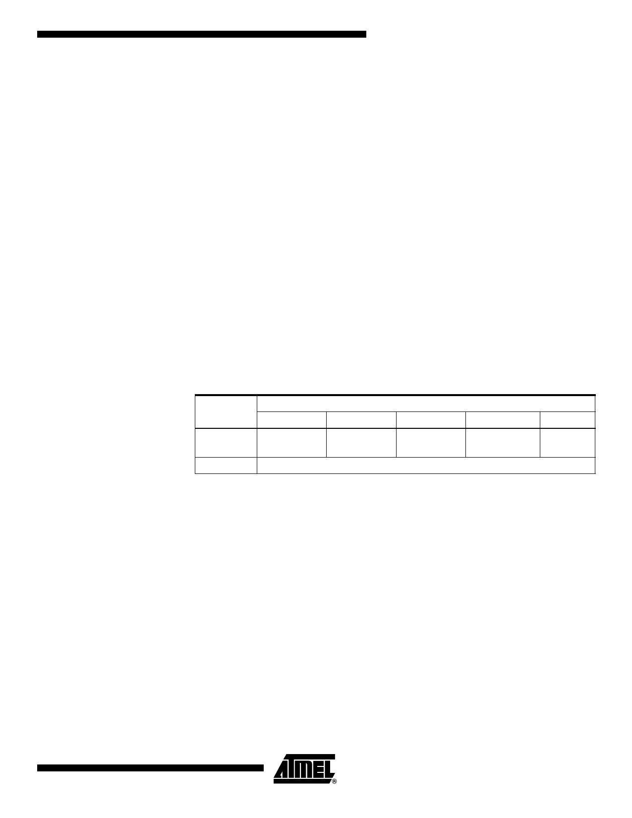
Table 2. Write Protect
WP Pin
Status
At VCC
At GND
Part of the Array Protected
24C01A
24C02
24C04
24C08A
Full (1K)
Array
Full (2K)
Array
Full (4K)
Array
Full (8K)
Array
Normal Read/Write Operations
24C16A
Full (16K)
Array
Memory Organization AT24C01A, 1K SERIAL EEPROM: Internally organized with 16 pages of 8 bytes each,
the 1K requires a 7-bit data word address for random word addressing.
AT24C02, 2K SERIAL EEPROM: Internally organized with 32 pages of 8 bytes each,
the 2K requires an 8-bit data word address for random word addressing.
AT24C04, 4K SERIAL EEPROM: Internally organized with 32 pages of 16 bytes each,
the 4K requires a 9-bit data word address for random word addressing.
AT24C08A, 8K SERIAL EEPROM: Internally organized with 64 pages of 16 bytes each,
the 8K requires a 10-bit data word address for random word addressing.
AT24C16A, 16K SERIAL EEPROM: Internally organized with 128 pages of 16 bytes
each, the 16K requires an 11-bit data word address for random word addressing.
3
0180V–SEEPR–8/05
Share Link: