AT25640B(2010) データシートの表示(PDF) - Atmel Corporation
部品番号
コンポーネント説明
メーカー
AT25640B Datasheet PDF : 26 Pages
| |||
Atmel AT25320B/640B
WRITE SEQUENCE (WRITE): In order to program the Atmel® AT25320B/640B, two separate instructions must be
executed. First, the device must be write enabled via the WREN instruction. Then a write (WRITE) instruction
may be executed. Also, the address of the memory location(s) to be programmed must be outside the protected
address field location selected by the block write protection level. During an internal write cycle, all commands will
be ignored except the RDSR instruction.
A write instruction requires the following sequence. After the CS line is pulled low to select the device, the WRITE
op-code is transmitted via the SI line followed by the byte address (A15–A0) and the data (D7–D0) to be pro-
grammed (see Table 3-6). Programming will start after the CS pin is brought high. The low-to-high transition of the
CS pin must occur during the SCK low-time immediately after clocking in the D0 (LSB) data bit.
The READY/BUSY status of the device can be determined by initiating a read status register
(RDSR) instruction. If Bit 0 = “1”, the write cycle is still in progress. If Bit 0 = “0”, the write cycle has ended. Only the
RDSR instruction is enabled during the write programming cycle.
The AT25320B/640B is capable of a 32-byte page write operation. After each byte of data is received, the five low-
order address bits are internally incremented by one; the high-order bits of the address will remain constant. If
more than 32-bytes of data are transmitted, the address counter will roll over and the previously written data will be
overwritten. The AT25320B/640B is automatically returned to the write disable state at the completion of a write
cycle.
Note: If the device is not write-enabled (WREN), the device will ignore the write instruction and will return to the standby
state, when CS is brought high. A new CS falling edge is required to reinitiate the serial communication.
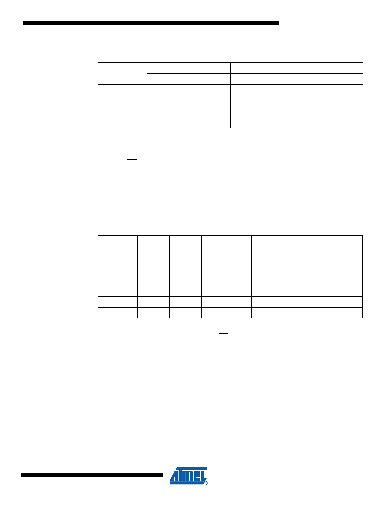
Table 3-6. Address Key
Address
AN
Don’t Care Bits
Atmel AT25320B
A11–A0
A15–A12
Atmel AT25640B
A12–A0
A15–A13
9
8535F–SEEPR–6/10
Share Link: 