NX25F641C データシートの表示(PDF) - NexFlash -> Winbond Electronics
部品番号
コンポーネント説明
メーカー
NX25F641C Datasheet PDF : 23 Pages
| |||
NX25F641C
Serial SRAM
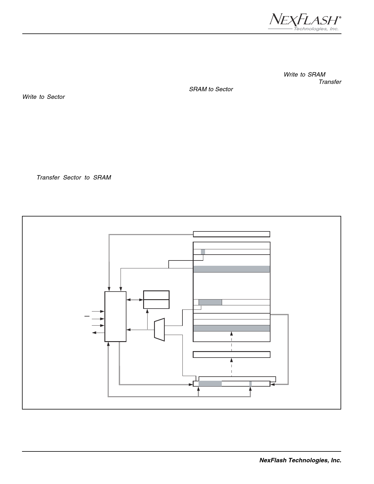
One of the most powerful features of the NX25F641C is
the integrated dual Serial SRAMs. The main purpose of
the Serial SRAMs is to serve as a buffer for sector data to
be written into the Serial Flash memory array. Using the
Write to Sector command, data is first shifted into the
SRAM from the SPI bus. When the command sequence
has been completed, the entire 528-bytes is written to the
selected sector. See Erase/Write cycle timing (tWP).
The SRAM is fully byte-addressable. Thus, the entire
528-bytes, a single byte, or a sequence of bytes can be
read from, or written to the SRAM. This allows the SRAM
to be used as a temporary work area for read-modify-write
operations prior to a sector write.
The Transfer Sector to SRAM command allows the
contents of a specified sector of Flash memory to be
moved to the SRAM (see figure 4). This can be useful
when only a portion of a sector needs to be altered. In this
case the sector is first transferred to the SRAM, where
modifications are made using the Write to SRAM com-
mand. Once modifications are completed, a Transfer
SRAM to Sector command is used to update the sector.
Using the SRAM Independent of Flash Memory
The SRAM can be used independently of Flash memory
operations for lookup tables, variable storage, or scratch
pad purposes. If the Flash memory needs to be written to
while SRAM is being used for a different purpose, the
contents can be temporarily stored to a sector and then
transferred back again when needed. The SRAM can be
especially useful for RAM-limited microcontroller-based
systems, eliminating the need for external SRAM and
freeing pins for other purposes. It can also make it possible
to use small pin-count microcontrollers, since only a few
pins are needed for the interface instead of the 20-40 pins
required for parallel bus-oriented Flash devices.
DEVICE INFORMATION SECTOR
READ FROM DEVICE
INFORMATION
SECTOR
READ FROM SECTOR
SCK
CS
SI
SO
SPI
COMMAND
AND
CONTROL
LOGIC
CONFIGURATION
REGISTER
STATUS
REGISTER
COMPARE SECTOR
TO SRAM
READ FROM
OR WRITE TO
SRAM
WRITE TO SECTOR
(VIA SRAM)
SERIAL FLASH MEMORY ARRAY
TRANSFER
SECTOR TO
SRAM
PAGE LATCH / BUFFER
TRANSFER
SRAM TO SECTOR
SERIAL SRAM
Figure 4. Command Relationships of the SPI Interface, Serial Flash Memory Array and SRAM
8
NexFlash Technologies, Inc.
PRELIMINARY NXSF032A-0502
05/06/02 ©
Share Link: 