NX25F641C-3T データシートの表示(PDF) - NexFlash -> Winbond Electronics
部品番号
コンポーネント説明
メーカー
NX25F641C-3T Datasheet PDF : 23 Pages
| |||
NX25F641C
Write Protection
The NX25F641C provide advanced software and hard-
ware write protection features. Software-controlled write
protection of the entire array is handled using the Write
Enable and Write Disable commands. Hardware write
protection is possible using the Write Protect pin (WP).
Write-protecting a portion of Flash memory is accommo-
dated by programming a write protect range in the
configuration register.
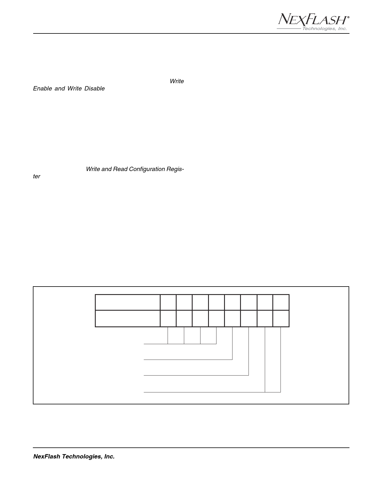
Configuration Register
The Configuration Register stores the current configura-
tion of the HOLD-R/B pin, read clock edge and write
protect range (Figure 5). The configuration register is
accessed using the Write and Read Configuration Regis-
ter commands. The non-volatile configuration register will
maintain its setting even when power is removed.
To avoid unnecessary programming of the configuration
register, and to save time during power-up, the
configuration register should be read upon power-up and
compared to the intended setting before sending a Write
Configuration Register command (Figure 5).
The factory default setting for the configuration register is
CF7-CF0 is: 0000 1001 B (write protect range = none,
read using falling edge of the clock, and pin 1 = no
connect). Bits CF15-CF8 are reserved. When writing to
the configuration register CF15-CF8 should be 0. When
reading, the settings of CF15-CF8 should be ignored.
Write Protect Range and Direction, WR[3:0], WD
The write protect range and direction bits WR[3:0] and
WD are located at configuration bits CF[7:4] and CF[3]
respectively. The write protect range and direction bits
select how the array is protected. They work in conjunc-
tion with the WP input pin, valid only if WP is inactive (high).
WR[3:0] can select write protection of all sectors, none of
the sectors, or specific sectors grouped in blocks of 64
(~32 KB). The WD bit specifies whether the protected block
range starts from the first sector, address 0 (000H), or
from the last sector (3FFF). Table 2 lists the write protect
sector range for the devices. Once protected, all further
writes to sectors within the range will be ignored. The fac-
tory default setting is with no write protected sectors,
WR=[0,0,0,0] and WD=1.
Read Clock Edge, RCE
The Read Clock Edge bit (RCE) is located at configura-
tion bit location CF[2]. It selects which edge of the clock
(SCK) is used while reading data out of the device.
Although the SPI protocol specifies that data is written
during the rising edge and read on the falling edge of the
clock, if required, the output can be driven on the rising
edge of the clock by setting the configuration registers
RCE bit to a 1. Using the rising edge of clock for reading
CF15:8
(RESERVED)
CF7 CF6 CF5 CF4 CF3 CF2 CF1 CF0
WR3 WR2 WR1 WR0 WD RCE HR1 HR0
WRITE PROTECT
RANGE
WRITE PROTECT
DIRECTION
READ DATA
CLOCK EDGE
HOLD-READY/BUSY
PIN FUNCTION
Figure 5. Configuration Register Bit Locations
NexFlash Technologies, Inc.
9
PRELIMINARY NXSF032A-0502
05/06/02 ©
Share Link: 