ATA06211D1C データシートの表示(PDF) - ANADIGICS
部品番号
コンポーネント説明
メーカー
ATA06211D1C Datasheet PDF : 8 Pages
| |||
ATA06211
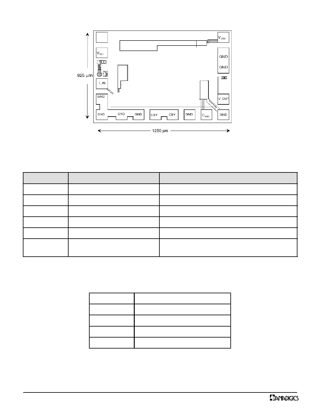
Figure 2: Bonding Pad Layout
PAD
VDD1
VDD2
IIN
VOUT
CAGC
CBY
Table 1: ATA06211D1C Pad Description
DESCRIPTION
COMMENT
VDD1
VDD2
TIA Input Current
Positive supply for input gain stage
Positive supply for second gain stage
Connect detector cathode for proper operation
TIA Output Voltage
Requires external DC block
External AGC Capacitor
Input Gain Stage Bypass
Capacitor
70K* CAGC = AGC Time Constant
>56 pF
ELECTRICAL CHARACTERISTICS
Table 2: Absolute Maximum Ratings
VDD1
7.0 V
VDD2
7.0 V
IIN
5 mA
TA
Operating Temp. - 40 °C to 125 °C
TS
Storage Temp. - 65 °C to 150 °C
Stresses in excess of the absolute ratings may cause
permanent damage. Functional operation is not
implied under these conditions. Exposure to absolute
ratings for extended periods of time may adversely
affect reliability.
2
PRELIMINARY DATA SHEET - Rev 4
08/2001
Share Link: 