ATA6613 データシートの表示(PDF) - Atmel Corporation
部品番号
コンポーネント説明
メーカー
ATA6613 Datasheet PDF : 364 Pages
| |||
ATA6612/ATA6613
3.3.20.1
3.3.20.2
Normal Mode
This is the normal transmitting and receiving mode at the LIN interface in accordance with the
LIN specification LIN 2.1. The voltage regulator is active and can source up to 50 mA. The
undervoltage detection is activated. The watchdog needs a trigger signal from NTRIG to avoid
resets at NRES. If NRES is switched to low, the IC changes its state to Fail-safe Mode.
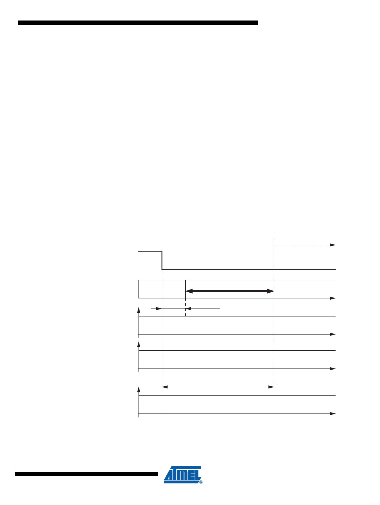
Silent Mode
A falling edge at EN when TXD is high switches the IC into Silent Mode. The TXD Signal has to
be logic high during the Mode Select window (see Figure 3-3 on page 11). The transmission
path is disabled in Silent Mode. The overall supply current from VBatt is a combination of the IVSsi
57 µA plus the VCC regulator output current IVCC.
The 3.3V/5V regulator with 2% tolerance can source up to 50 mA. The internal slave termination
between the LIN pin and the VS pin is disabled in Silent Mode, only a weak pull-up current
(typically 10 µA) between the LIN pin and the VS pin is present. Silent Mode can be activated
independently from the actual level on the LIN, WAKE, or KL_15 pins.
If an undervoltage condition occurs, NRES is switched to low, and the IC changes its state to
Fail-safe Mode.
A voltage less than the LIN Pre_Wake detection VLINL at the LIN pin activates the internal LIN
receiver and switches on the internal slave termination between the LIN pin and the VS pin.
Figure 3-3. Switch to Silent Mode
Normal Mode
Silent Mode
EN
TXD
NRES
Mode select window
td = 3.2 µs
VCC
LIN
Delay time silent mode
td_sleep = maximum 20 µs
LIN switches directly to recessive mode
11
9111G–AUTO–05/10
Share Link: 