ATA6628 データシートの表示(PDF) - Atmel Corporation
部品番号
コンポーネント説明
メーカー
ATA6628 Datasheet PDF : 36 Pages
| |||
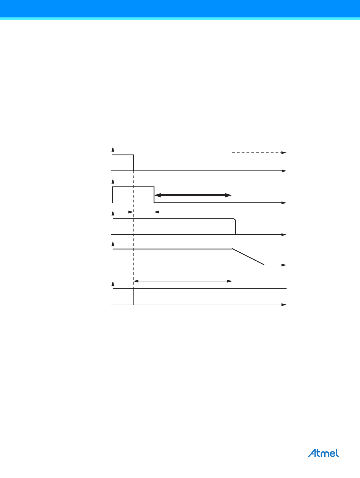
4.3 Sleep Mode
A falling edge at EN when TXD is low switches the IC into Sleep Mode. The TXD Signal has to be logic low during the Mode
Select window (Figure 4-4 on page 10). In order to avoid any influence to the LIN-pin during switching into sleep mode it is
possible to switch the EN up to 3.2µs earlier to Low than the TXD. The best and easiest way are two falling edges at TXD
and EN at the same time. The transmission path is disabled in Sleep Mode. The supply current IVSsleep from VBatt is typically
10µA.
The INH output, the PV output and the VCC regulator are switched off. NRES and RXD are low. The internal slave
termination between the LIN pin and VS pin is disabled to minimize the current consumption in the event that the LIN pin is
short-circuited to GND. Only a weak pull-up current (typically 10µA) between the LIN pin and the VS pin is present. Sleep
Mode can be activated independently from the current level on the LIN, WAKE, or KL_15 pin.
A voltage less than the LIN Pre_Wake detection VLINL at the LIN pin activates the internal LIN receiver and starts the wake-
up detection timer.
Figure 4-4. Switch to Sleep Mode
Normal Mode
Sleep Mode
EN
TXD
NRES
VCC
LIN
Mode select window
td = 3.2μs
Delay time sleep mode
td_sleep = maximum 20μs
LIN switches directly to recessive mode
10 ATA6628/ATA6630 [DATASHEET]
9117I–AUTO–10/14
Share Link: 