ATA6630 データシートの表示(PDF) - Atmel Corporation
部品番号
コンポーネント説明
メーカー
ATA6630 Datasheet PDF : 36 Pages
| |||
4.5 Fail-safe Mode
The device automatically switches to Fail-safe Mode at system power-up. The voltage regulator is switched on (see Figure
5-1 on page 18). The NRES output remains low for tres = 4ms and gives a reset to the microcontroller. LIN communication is
switched off. The IC stays in this mode until EN is switched to high. The IC then changes to Normal Mode. A power down of
VBatt (VS < VSthU) during Silent or Sleep Mode switches the IC into Fail-safe Mode after power up. A low at NRES switches
into Fail-safe Mode directly. During Fail-safe Mode, the TXD pin is an output and signals the fail-safe source. The watchdog
is switched on.
The LIN SBC can operate in different Modes, like Normal, Silent, or Sleep Mode. The functionality of these modes is
described in Table 4-2.
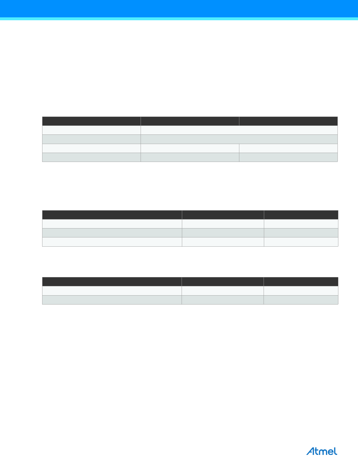
Table 4-2. TXD, RXD Depending from Operation Modes
Different Modes
Fail-safe Mode
Normal Mode
Silent Mode
Sleep Mode
TXD
RXD
Signalling fail-safe sources (see Table 4-3 and Table 4-4)
Follows data transmission
High
High
Low
Low
A wake-up event from either Silent or Sleep Mode will be signalled to the microcontroller using the two pins RXD and TXD.
The coding is shown in Table 4-3.
A wake-up event will switch the IC to the Fail-safe Mode.
Table 4-3. Signalling Fail-safe Sources
Fail-safe Sources
LIN wake-up (pin LIN)
Local wake-up (at pin Wake, pin KL15)
VSth (battery) undervoltage detection
TXD
Low
Low
High
RXD
Low
High
Low
Table 4-4. Signalling in Fail-safe Mode after Reset (NRES was Low), Shows the Reset Source at TXD and RXD
Pins
Fail-safe Sources
VCC undervoltage at NRES
Watchdog reset at NRES
TXD
High
High
RXD
Low
High
14 ATA6628/ATA6630 [DATASHEET]
9117I–AUTO–10/14
Share Link: 