ATA6662 データシートの表示(PDF) - Atmel Corporation
部品番号
コンポーネント説明
メーカー
ATA6662 Datasheet PDF : 18 Pages
| |||
ATA6662
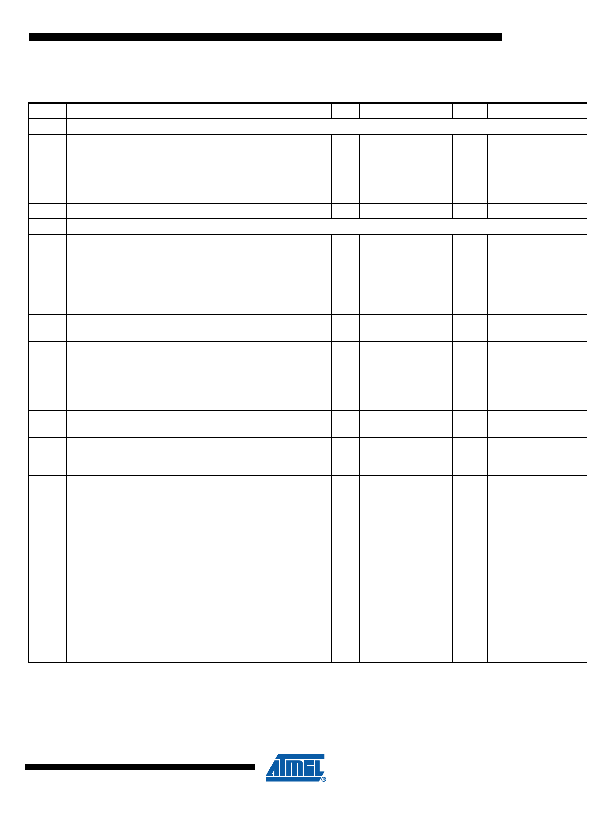
6. Electrical Characteristics (Continued)
5V < VS < 27V, Tj = –40°C to +150°C
No. Parameters
Test Conditions
Pin Symbol Min. Typ. Max.
6 WAKE Pin
6.1 High-level input voltage
3
VWAKEH
VS –
1V
VS +
0.3V
6.2 Low-level input voltage
IWAKE = Typically –3 µA
3
VWAKEL
–1V
VS –
3.3V
6.3 Wake pull-up current
6.4 High-level leakage current
7 LIN Bus Driver
VS < 27V
VS = 27V, VWAKE = 27V
3
IWAKE
–30 –10
3
IWAKE
–5
+5
7.1 Driver recessive output voltage RLOAD = 500Ω / 1 kΩ
6
VBUSrec
0.9 ×
VS
VS
7.2
Driver dominant voltage
VBUSdom_DRV_LoSUP
VVS = 7V, Rload = 500Ω
6
V_LoSUP
1.2
7.3
Driver dominant voltage
VBUSdom_DRV_HiSUP
VVS = 18V, Rload = 500Ω
6
V_HiSUP
2
7.4
Driver dominant voltage
VBUSdom_DRV_LoSUP
VVS = 7V, Rload = 1000Ω
6
V_LoSUP_1k
0.6
7.5
Driver dominant voltage
VBUSdom_DRV_HiSUP
VVS = 18V, Rload = 1000Ω
6
V_HiSUP_1k_
0.8
7.6 Pull-up resistor to VS
The serial diode is mandatory 6
RLIN
20
30
60
7.7
Voltage drop at the serial diodes
In pull-up path with Rslave
ISerDiode = 10 mA
6
VSerDiode
0.4
1.0
7.8
LIN current limitation
VBUS = VBAT_max
6
IBUS_LIM
40 120 200
Input leakage current at the
Input leakage current
7.9 receiver, including pull-up
resistor as specified
Driver off
VBUS = 0V, VS = 12V
6 IBUS_PAS_dom
–1
Driver off
7.10
Leakage current LIN recessive
8V < VBAT < 18V
8V < VBUS < 18V
VBUS ≥ VBAT
6
IBUS_PAS_rec
10
20
Leakage current at ground loss;
7.11
Control unit disconnected from GNDDevice = VS
ground; Loss of local ground
VBAT =12V
must not affected communication 0V < VBUS < 18V
in the residual network
6 IBUS_NO_gnd –10
+0.5 +10
Leakage current at loss of
7.12
battery; Node has to substain the VBAT disconnected
current that can flow under this VSUP_Device = GND
condition; Bus must remain
0V < VBUS < 18V
operational under this condition
6
IBUS_NO_bat
0.1
2
7.13 Capacitance on pin LIN to GND
6
CLIN
20
*) Type means: A = 100% tested, B = 100% correlation tested, C = Characterized on samples, D = Design parameter
Unit Type*
V
A
V
A
µA A
µA A
V
A
V
A
V
A
V
A
V
A
kΩ A
V
D
mA A
mA A
µA A
µA A
µA A
pF D
11
4916O–AUTO–05/10
Share Link: 