ATA12001 データシートの表示(PDF) - ANADIGICS
部品番号
コンポーネント説明
メーカー
ATA12001 Datasheet PDF : 8 Pages
| |||
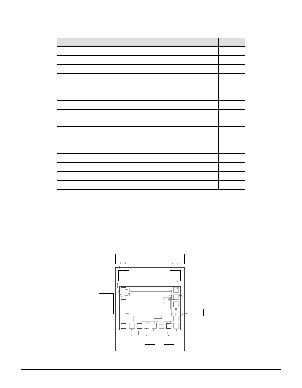
Table 3: Electrical Specifications (1)
(TA = 25°C, VDD =+5.0V + 10%, CDIODE + CSTRAY = 0.5 pF, Det. cathode to IIN)
PARAMETER
Transresistance (RL= ¥ ,IDC<500nA)
Transresistance (RL=50W) (1)
Bandwidth -3dB
MIN TYP MAX UNIT
3.5
KW
1.2
1.4
KW
900 1100
MHz
Input Resistance (2)
100
W
Output Resistance
30
50
60
W
Supply Current
15
30
45
mA
Input Offset Voltage
1.4
1.6
1.9
Volts
Output Offset Voltage
1.8
Volts
AGC Threshold (IIN) (3)
Optical Overload (4)
100 150
-3
0
mA
dBm
Input Noise Current (5)
120 170
nA
AGC Time Constant (6)
16
m sec
Offset Voltage Drift
±1
mV/ ºC
Optical Sensitivity (7)
-29
-31
dBm
Operating Voltage Range
+ 4.5 + 5.0 + 6.0 Volts
Operating Temperature Range
- 40
85
ºC
Notes:
1. f = 50MHz
2. Measured with Iin below AGC Threshold. During AGC, input impedance will
decrease proportionally to Iin.
3. Defined as the Iin where Transresistance has decreased by 50%.
4. See note on Indirect Measurement of Optical Overload.
5. See note on Measurement of Input Referred Noise Current.
6. CAGC = 220 pF
7. Parameter is guaranteed (not tested) by design and characterization data
@ 1.2 Gb/s, assuming dectector responsivity of 0.9.
VDD
ATA12001
PIN
56pF
GND
56pF
VDD2
VDD1
4E
IIN
GND
GND
1992
GND
VOUT
GND GND GND CBY CBY GND CAGC GND
56pF
56pF
OUT
Figure 3: ATA 12001 Typical Bonding Diagram
PRELIMINARY DATA SHEET - Rev 4
3
08/2001
Share Link: 