ATA12001 データシートの表示(PDF) - ANADIGICS
部品番号
コンポーネント説明
メーカー
ATA12001 Datasheet PDF : 8 Pages
| |||
ATA12001
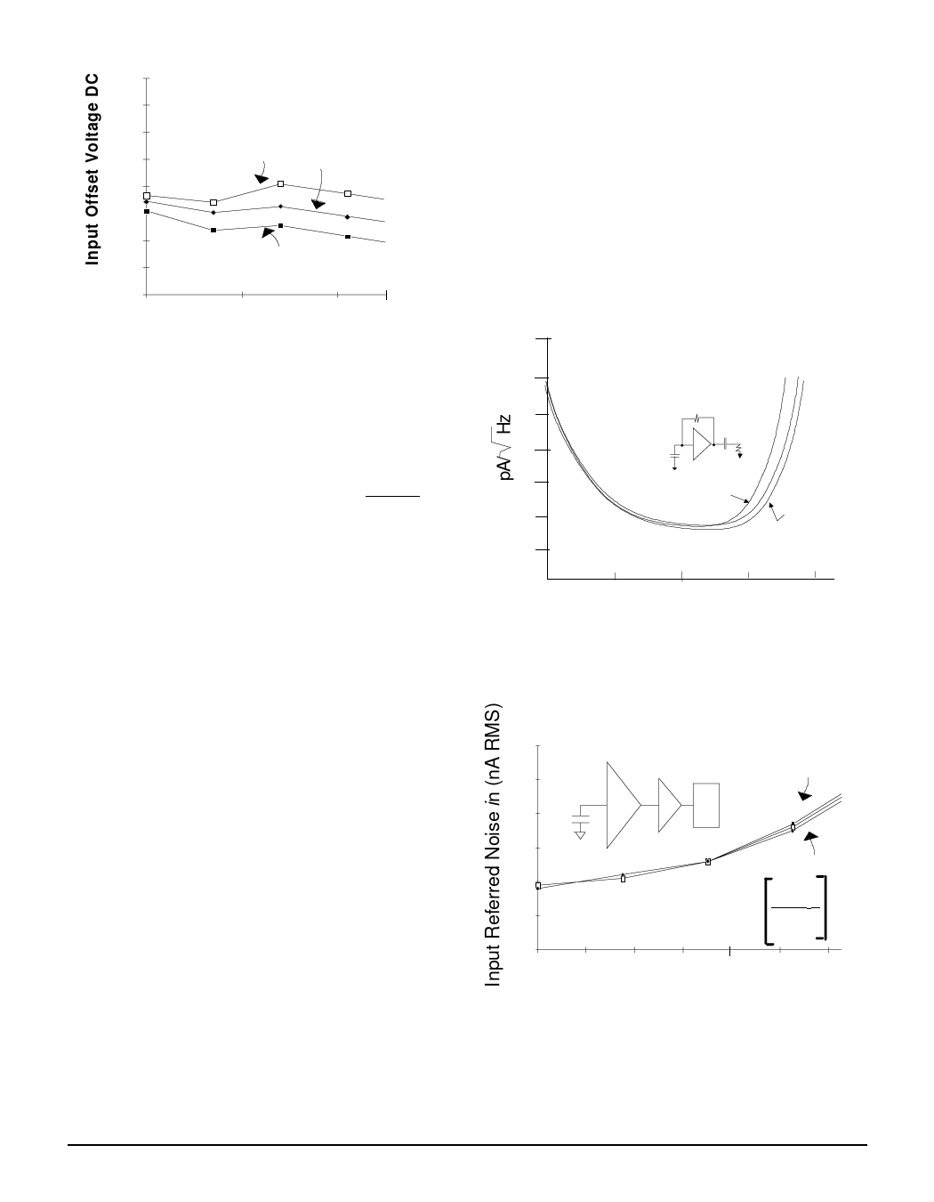
1.9
1.85
1.8
1.75
1.7
1.65
1.6
1.55
1.5
VDD = 5.5 V VDD = 5.0V
VDD = 4.5V
- 40
10
60
85
Temperature (C)
Figure 9: Input Offset Voltage vs. Temperature
CBY Connection
The CBY pad must be connected via a low inductance
path to a surface mount capacitor of at least 56 pF
(additional capacitance can be added in parallel with
the 56 pF or 220 pF capacitors to improve low
frequency response and noise performance).
Referring to the equivalent circuit diagram and the
typical bonding diagram, it is critical that the
connection from CBY to the bypass capacitor use
two bond wires for low inductance, since any high
frequency impedance at this node will be fed back to
the open loop amplifier with a resulting loss of
transimpedance bandwidth. Two pads are provided
for this purpose.
Sensitivity and Bandwidth
In order to guarantee sensitivity and bandwidth
performance, the TIA is subjected to a
comprehensive series of tests at the die sort level
(100% testing at 25 oC) to verify the DC parametric
performance and the high frequency performance
(i.e. adequate |S21|) of the amplifier. Acceptably high
|S21| of the internal gain stages will ensure low
amplifier input capacitance and hence low input
referred noise current. Transimpedance sensitivity
and bandwidth are then guaranteed by design and
correlation with RF and DC die sort test results.
ndirect Measurement of Optical Overload
Optical overload can be defined as the maximum
optical power above which the BER (bit error rate)
increases beyond 1 error in 1010 bits. The
ATA12001D1C is 100% tested at die sort by a DC
measurement which has excellent correlation with
an PRBS optical overload measurement. The
measurement consists of sinking a negative current
(see VOUT vs IIN figure) from the TIA and determining
the point of output voltage collapse. Also the input
node virtual ground during heavy AGC is checked
to verify that the linearity (i.e. pulse width distortion)
of the amplifier has not been compromised.
Measurement of Input Referred Noise Current
The Input Noise Current is directly related to
sensitivity . It can be defined as the output noise
voltage (Vout), with no input signal, (including a 1
GHz lowpass filter at the output of the TIA) divided by
the AC transresistance.
10
9
8
7
RF
50Ω
6
CT
5
CT = 1.0pF
4
CT = 0.5pF
3
-0.1
1
10
100
1000
Figure 10: Input Referred Noise Spectral Density
Input referred noise test circuit
16
15
14 0.5pF
25dB
100
TIA
MHz
LPF
VDD = 4.5 V
13
VDD = 5.5V
12
11
η(dBm) = 10 LOG
6500in
R
10
-40
0 40 80
Temperature (OC)
FIgure 11: Input Referred Noise vs Temperature
6
PRELIMINARY DATA SHEET - Rev 4
08/2001
Share Link: 