AWC6340Q7 データシートの表示(PDF) - ANADIGICS
部品番号
コンポーネント説明
メーカー
AWC6340Q7 Datasheet PDF : 10 Pages
| |||
FEATURES
• CDMA/EVDO Compliant
• HELPTM technology
• High Efficiency (RC-1 waveform):
• 36 % @ POUT = +28.0 dBm
• 16 % @ POUT = +15 dBm
• Low Quiescent Current: 12 mA
• Low Leakage Current in Shutdown Mode: <5 µA
• Internal Voltage Regulator
• Integrated “daisy chainable” directional coupler
with CPLIN and CPLOUT port.
• Internal DC Blocks on all RF ports
• Optimized for a 50 Ω System
• 1.8V Control Logic
• RoHS Compliant Package, 260 oC MSL-3
AWC6340
HELPTM CDMA Band Class 0,10
CDMA Power Amplifier Module
PRELIMINARY DATA SHEET- Rev 1.8
AWC6340
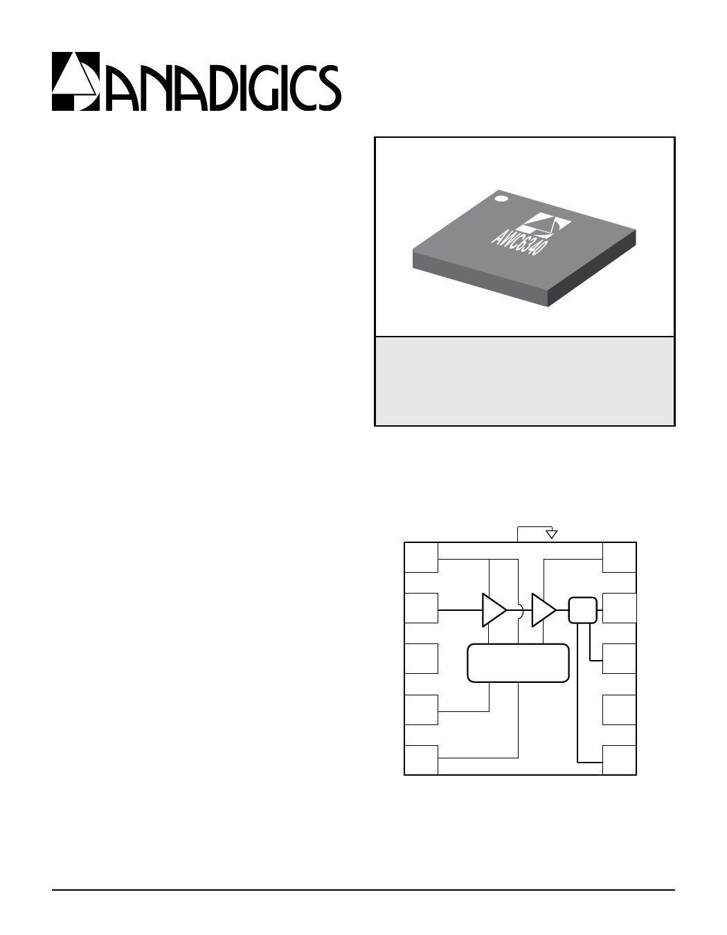
M45 Package
10 Pin 3 mm x 3 mm x 1 mm
Surface Mount Module
APPLICATIONS
• Band Class 0, 10 CDMA/EVDO Wireless
Devices
PRODUCT DESCRIPTION
The AWC6340 is a HELPTM product for CDMA
devices operating in Band Class 0 and 10. This PA
VBATT
1
incorporates ANADIGICS’ HELP™ technology to
deliver exceptional efficiency at low power levels and
low quiescent current without the need for external
RFIN 2
voltage regulators or converters. The device is
manufactured using advanced InGaP HBT technology
offering state-of-the-art reliability, temperature stability, GND 3
and ruggedness. Two selectable bias modes that
optimize efficiency for different output power levels and
a shutdown mode with low leakage current increase VMODE 4
handset talk and standby time. A “daisy chainable”
directional coupler is integrated in the module thus
eliminating the need of an external coupler. The
self-contained 3 mm x 3 mm x 1 mm surface mount
VEN 5
package incorporates matching networks optimized for
output power, efficiency, and linearity in a 50 Ω system.
GND at Slug (pad)
10 VCC
CPL
9
RFOUT
Bias Control
Voltage Regulation
8 CPLIN
7 GND
6 CPLOUT
Figure 1: Block Diagram
02/2012
Share Link: 