AWC6340P9 データシートの表示(PDF) - ANADIGICS
部品番号
コンポーネント説明
メーカー
AWC6340P9 Datasheet PDF : 10 Pages
| |||
AWC6340
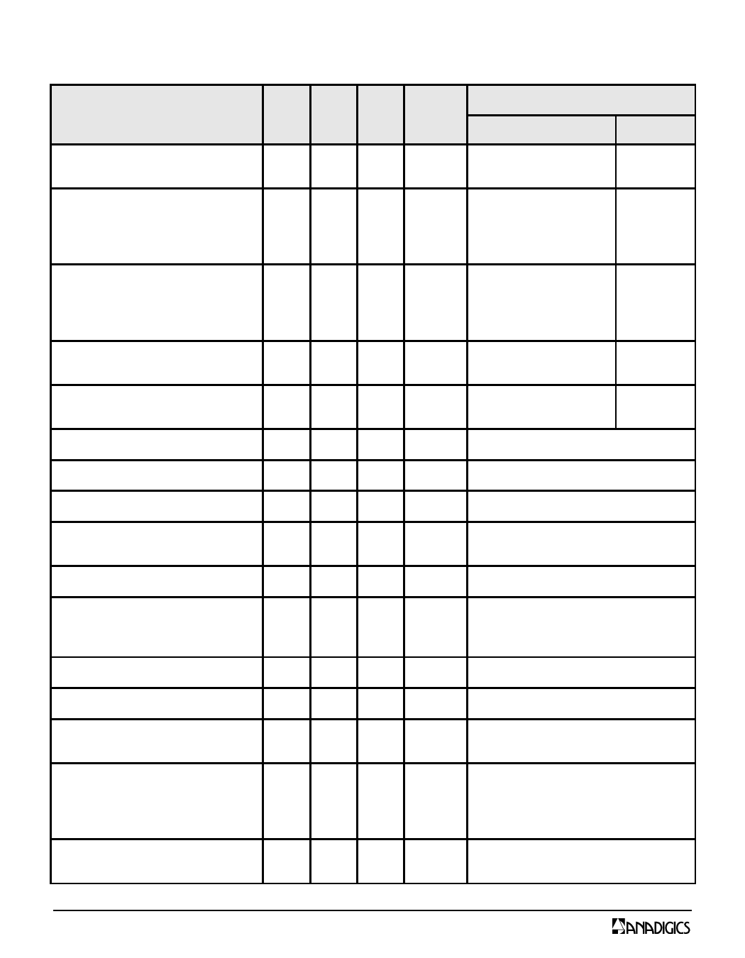
Table 4: Electrical Specifications - CDMA2000 Operation (RC-1 waveform)
(TC = +25 °C, VBATT = VCC = +3.4 V, VENABLE = +1.8 V, 50 Ω system)
PARAMETER
MIN TYP MAX
UNIT
COMMENTS
POUT
VMODE
Gain
-
28
-
- 15.5 -
dB
+28 dBm
+15 dBm
0V
1.8 V
Adjacent Channel Power
at ±885 kHz offset (1)
-
-50
-
Primary Channel BW = 1.23 MHZ -
-49
-
Adjacent Channel BW = 30 kHz
dBc
+28 dBm
+15 dBm
0V
1.8 V
Adjacent Channel Power
at ±1.98 MHz offset (1)
-
-62
-
Primary Channel BW = 1.23 MHZ -
-58
-
Adjacent Channel BW = 30 kHz
dBc
+28 dBm
+15 dBm
0V
1.8 V
Power-Added Efficiency (1)
-
36
-
-
16
-
%
+28 dBm
+15 dBm
0V
1.8 V
Quiescent Current (Icq)
Low Bias Mode
-
12
-
mA through VCC pin
1.8 V
Mode Control Current
-
0.06 0.15
mA through VMODE pin, VMODE = 1.8 V
Enable Current
-
0.4 0.6
mA through VEN pin
BATT Current
-
3.0 0.5
mA through VBATT pin, VMODE = +1.8 V
Leakage Current
-
<5
-
µA
VBATT = +4.35 V, VCC = +4.35 V,
VEN = 0 V, VMODE = 0 V
Noise in Receive Band
- -135 - dBm/Hz
Harmonic
2fo
3fo, 4fo
-
-40
-
-
-60
-
dBc POUT ≤ +28 dBm
Coupling Factor
-
20
-
dB
Directivity
-
20
-
dB
Coupler IN_OUT
Daisy Chain Insertion Loss
- <0.25 -
dB
698 MHz to 2620 MHz
Pin 8-6, Shutdown Mode
Spurious Output Level
(all spurious outputs)
POUT ≤ +28 dBm
-
-
-70
dBc
In-band Load VSWR < 5:1
Out-of-band Load VSWR < 10:1
Applies over all operating conditions
Load mismatch stress with no
permanent degradation or failure
8:1
-
- VSWR Applies over all operating conditions
Notes:
(1) ACLR and Efficiency measured at 836.5 MHz.
4
PRELIMINARY DATA SHEET - Rev 1.8
02/2012
Share Link: 