AWT6132RM5P9 データシートの表示(PDF) - ANADIGICS
部品番号
コンポーネント説明
メーカー
AWT6132RM5P9 Datasheet PDF : 8 Pages
| |||
ELECTRICAL CHARACTERISTICS
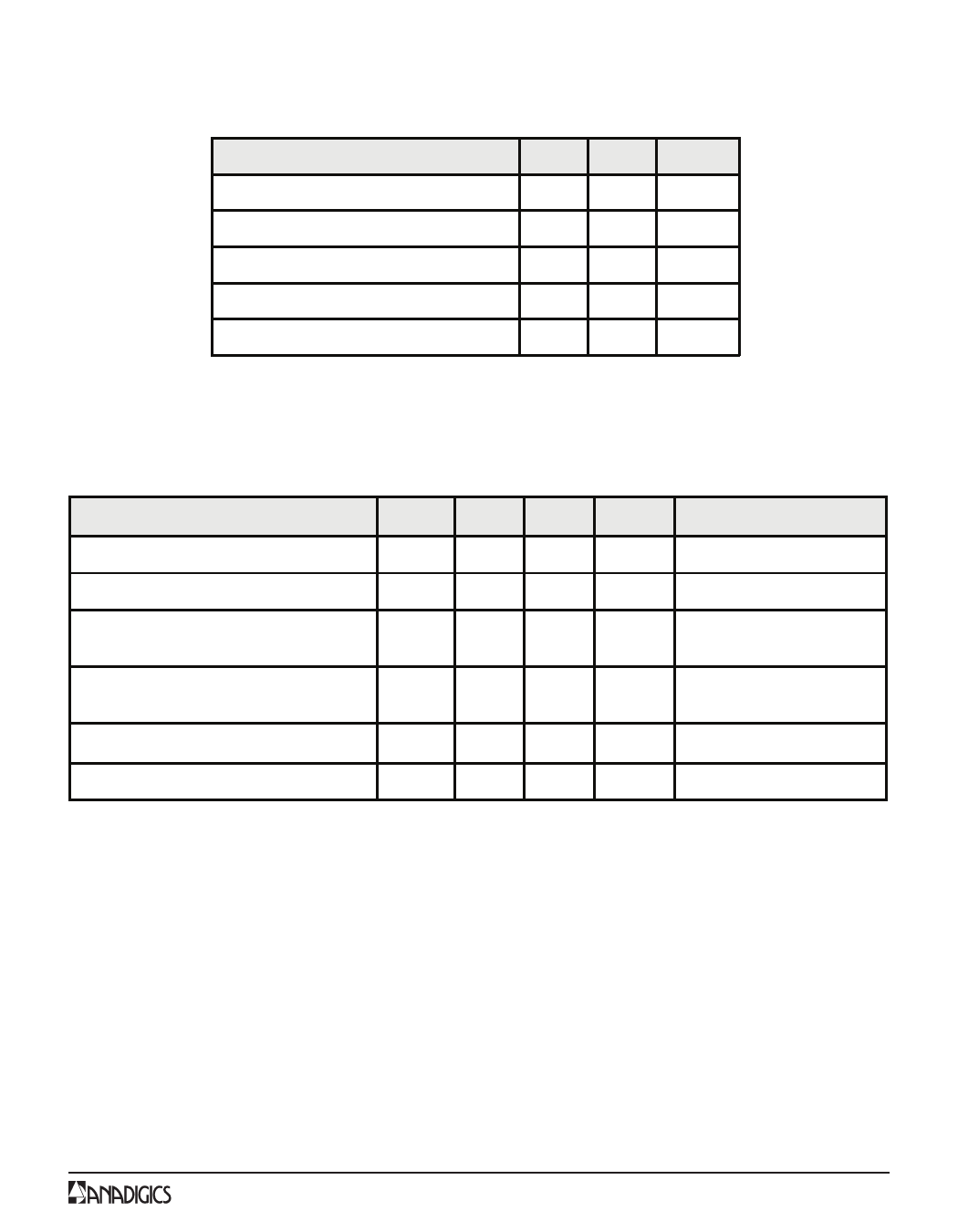
Table 2: Absolute Minimum and Maximum Ratings
PARAMETER
MIN MAX UNIT
Supply Voltage (VCC )
0
+5
V
Mode Control Voltage (VMODE)
0
+3.4
V
Reference Voltage (VREF)
0
+3.4
V
RF Input Power (PIN)
-
+10
dBm
Storage Temperature (TSTG)
-40 +150
°C
Stresses in excess of the absolute ratings may cause permanent damage.
Functional operation is not implied under these conditions. Exposure
to absolute ratings for extended periods of time may adversely affect
reliability.
AWT6132R
PARAMETER
Table 3: Operating Ranges
MIN TYP MAX
UNIT
COMMENTS
Operating Frequency (f)
410
-
420
MHz
Supply Voltage (VCC)
+3.2 +3.4 +4.2
V
Reference Voltage (VREF)
+2.80 +2.90 +3.1
0
-
+0.5
V
PA"on"
PA"shut down"
Mode Control Voltage (VMODE)
+2.5 +2.90 +3.1
0
-
+0.5
V
Low Bias Mode
High Bias Mode
RF Output Power (POUT)
+29.0 (1) +29.5
-
dBm CDMA, VCC =+3.4V
Case Temperature (TC)
-30
-
+90
oC
The device may be operated safely over these conditions; however, parametric performance is guaranteed only
over the conditions defined in the electrical specifications.
Notes:
(1) For operation at Vcc = +3.2 V , POUT is derated by 0.5 dB.
MASTER DATA SHEET - Rev 2.1
3
10/2008
Share Link: 